
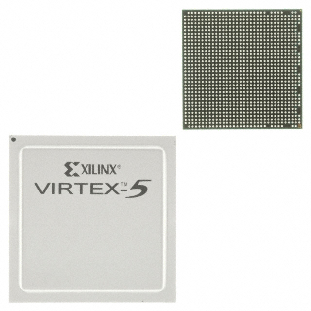
XC5VLX110T-1FFG1136CES
| Part Description |
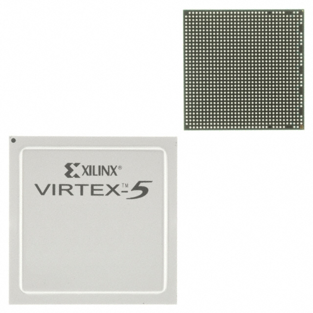
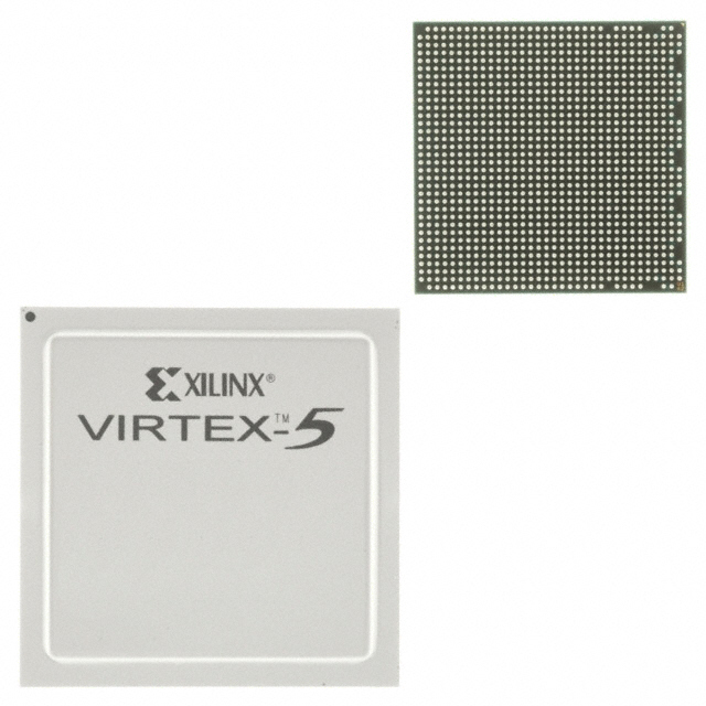
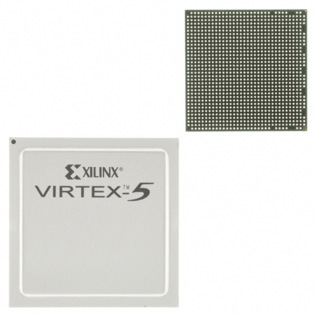
Virtex®-5 LXT Field Programmable Gate Array (FPGA) IC 640 5455872 110592 1136-BBGA, FCBGA |
|---|---|
| Quantity | 1,009 Available (as of October 8, 2026) |
| Product Category | Field Programmable Gate Array (FPGA) |
|---|---|
| Manufacturer | AMD |
| Manufacturing Status | Obsolete |
| Manufacturer Standard Lead Time | Contact Us |
| Datasheet |
Specifications & Environmental
| Device Package | 1136-FCBGA (35x35) | Grade | Commercial | Operating Temperature | 0°C – 85°C | ||
|---|---|---|---|---|---|---|---|
| Package / Case | 1136-BBGA, FCBGA | Number of I/O | 640 | Voltage | 950 mV - 1.05 V | ||
| Mounting Method | Surface Mount | RoHS Compliance | Unknown | REACH Compliance | REACH Unaffected | ||
| Moisture Sensitivity Level | 4 (72 Hours) | Number of LABs/CLBs | 8640 | Number of Logic Elements/Cells | 110592 | ||
| Number of Gates | N/A | ECCN | 3A001A7A | HTS Code | 8542.39.0001 | ||
| Qualification | N/A | Total RAM Bits | 5455872 |
Overview of XC5VLX110T-1FFG1136CES – Virtex®-5 LXT Field Programmable Gate Array
The XC5VLX110T-1FFG1136CES is a Virtex®-5 LXT Field Programmable Gate Array (FPGA) offered in a 1136-FCBGA package for surface-mount applications. It delivers a large logic capacity and on-chip memory with extensive I/O capability, targeted at commercial-grade programmable logic designs that require significant logic resources and high pin counts.
Key hardware characteristics include 110,592 logic elements, approximately 5.46 Mbits of embedded memory, up to 640 I/O, a 1136-FCBGA (35×35 mm) package, and a core voltage range of 0.95–1.05 V, with an operating temperature range of 0 °C to 85 °C.
Key Features
- Logic Capacity 110,592 logic elements (8,640 CLBs) to implement large digital designs and complex logic functions.
- Embedded Memory Approximately 5.46 Mbits of on-chip RAM for data buffering, FIFOs, and state storage without external memory.
- I/O Resources Up to 640 I/O pins to support high-density interfacing and multiple parallel connections.
- Power and Voltage Core supply voltage range of 0.95–1.05 V, allowing precise power design around the FPGA core rails.
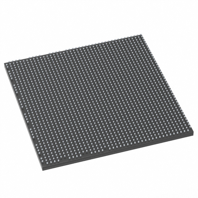
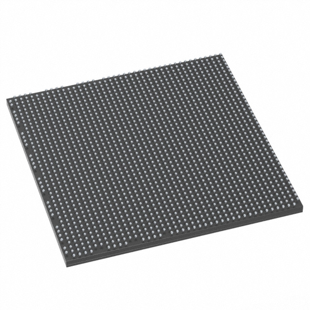
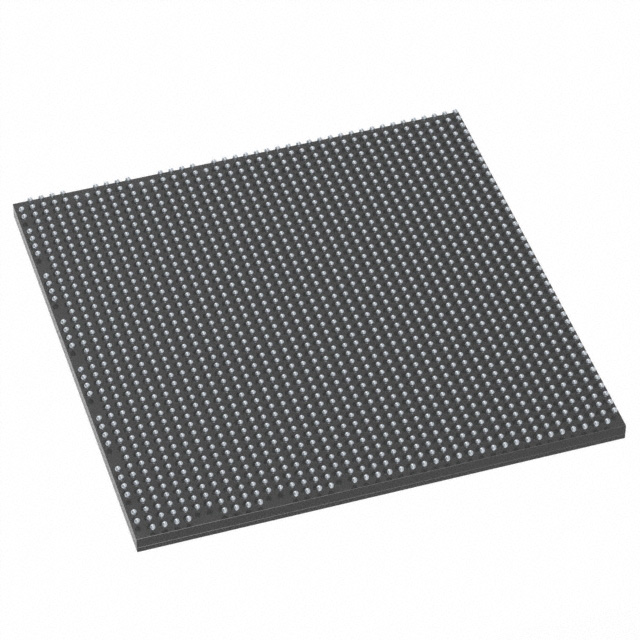
- Package and Mounting 1136-BBGA / 1136-FCBGA (35×35 mm) ball-grid array package, designed for surface-mount PCB assembly.
- Operating Range Commercial-grade operation from 0 °C to 85 °C for standard temperature environments.
- Environmental Compliance RoHS compliant to meet common lead-free assembly requirements.
Typical Applications
- Programmable Logic and Prototyping Use the device to implement and iterate large, custom digital logic designs during development and prototyping phases.
- High-Density I/O Systems Leverage the up to 640 I/O pins for designs requiring many parallel interfaces or complex board-level connectivity.
- Memory-Intensive Designs Embedded memory (approximately 5.46 Mbits) supports buffering, packet staging, and intermediate data storage within the FPGA fabric.
Unique Advantages
- Large Logic Resource: 110,592 logic elements enable implementation of sizable and complex logic networks without partitioning across multiple devices.
- Significant On-Chip Memory: Approximately 5.46 Mbits of embedded RAM reduces dependence on external memory for many common buffering and state-storage tasks.
- Extensive I/O Capability: Up to 640 I/O pins support high pin-count designs and simplify board-level integration with multiple peripherals.
- Compact BGA Packaging: 1136-FCBGA (35×35 mm) provides a high-density package suitable for surface-mount assembly while consolidating pins in a single footprint.
- Commercial-Grade Operation: Rated for 0 °C to 85 °C, matching typical commercial-environment deployment requirements.
- RoHS Compliant: Meets lead-free manufacturing standards for environmental compliance in mainstream production.
Why Choose XC5VLX110T-1FFG1136CES?
The XC5VLX110T-1FFG1136CES positions itself as a robust commercial-grade FPGA option for designs that demand substantial logic capacity, embedded memory, and high I/O counts within a single 1136-FCBGA package. Its combination of 110,592 logic elements and approximately 5.46 Mbits of on-chip RAM supports consolidated, high-density digital designs and system-level integration.
This device suits engineering teams and procurement groups seeking a programmable logic solution that balances large resource counts, a compact BGA footprint, and RoHS compliance for standard commercial applications. It provides scalability for complex designs while aligning with common power and temperature design constraints.
If you would like pricing or availability, request a quote or submit a quote inquiry to receive further purchasing details and lead-time information.





















Date Founded: 1969
Headquarters: Santa Clara, California, USA
Employees: 25,000+
Revenue: $22.68 Billion
Certifications and Memberships: ISO9001:2015, RoHS, REACH











