
XC7A100T-2FGG676C
| Part Description |
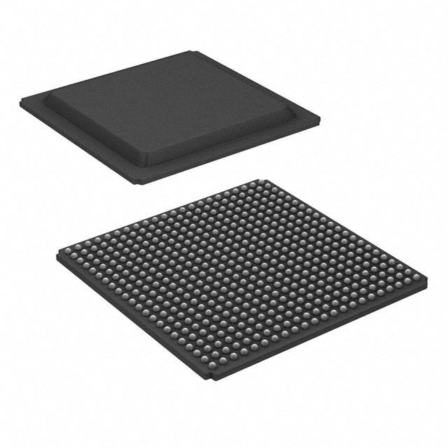
Artix-7 Field Programmable Gate Array (FPGA) IC 300 4976640 101440 676-BGA |
|---|---|
| Quantity | 908 Available (as of June 15, 2026) |

| Product Category | Field Programmable Gate Array (FPGA) |
|---|---|
| Manufacturer | AMD |
| Manufacturing Status | Active |
| Manufacturer Standard Lead Time | 16 Weeks |
| Datasheet |
Specifications & Environmental
| Device Package | 676-FBGA (27x27) | Grade | Commercial | Operating Temperature | 0°C – 85°C | ||
|---|---|---|---|---|---|---|---|
| Package / Case | 676-BGA | Number of I/O | 300 | Voltage | 950 mV - 1.05 V | ||
| Mounting Method | Surface Mount | RoHS Compliance | ROHS3 Compliant | REACH Compliance | REACH Unaffected | ||
| Moisture Sensitivity Level | 3 (168 Hours) | Number of LABs/CLBs | 7925 | Number of Logic Elements/Cells | 101440 | ||
| Number of Gates | N/A | ECCN | 3A991D | HTS Code | 8542.39.0001 | ||
| Qualification | N/A | Total RAM Bits | 4976640 |
Overview of XC7A100T-2FGG676C – Artix-7 Field Programmable Gate Array (FPGA) IC 300 4976640 101440 676-BGA
The XC7A100T-2FGG676C is an Artix-7 Field Programmable Gate Array (FPGA) offering a high logic element count and substantial on-chip memory in a compact BGA package. It provides 101,440 logic elements, approximately 4.98 Mbits of embedded memory, and 300 user I/O pins to support dense, board-level programmable logic implementations.
Designed as a commercial-grade, surface-mount FPGA, this device operates from a core voltage of 0.95 V to 1.05 V and is specified for operation from 0 °C to 85 °C. The 676-FBGA (27×27) package enables space-efficient integration on moderately constrained PCBs.
Key Features
- Core Logic 101,440 logic elements for implementing complex digital designs and flexible hardware acceleration.
- Embedded Memory Approximately 4.98 Mbits of on-chip RAM to support buffering, packet processing, and local data storage.
- I/O Capacity 300 user I/O pins provide broad interfacing capability for peripherals, sensors, and external devices.
- Power Supply Core voltage range of 0.95 V to 1.05 V to match low-voltage FPGA power domains and designs.
- Package & Mounting 676-FBGA (27×27) package in a surface-mount form factor for compact board integration.
- Operating Range & Grade Commercial grade device specified for 0 °C to 85 °C operation.
- Standards Compliance RoHS compliant for reduced hazardous substance content.
Typical Applications
- Programmable Logic and Prototyping Use the FPGA’s 101,440 logic elements and reprogrammable nature for hardware prototyping and iterative design validation.
- Data Buffering and On‑chip Storage Approximately 4.98 Mbits of embedded memory supports buffering and local data handling in packet or stream processing tasks.
- High‑density I/O Interfaces With 300 I/O pins, the device is suited for applications requiring multiple peripheral interfaces or parallel signal connectivity.
- Space‑constrained Board Designs The 676-FBGA (27×27) surface-mount package enables compact integration on PCBs where board area is limited.
Unique Advantages
- High Logic Capacity: 101,440 logic elements enable implementation of sizable custom logic blocks and mixed-function designs without external gate arrays.
- Substantial On‑chip Memory: Approximately 4.98 Mbits of embedded RAM reduces reliance on external memory for many buffering and state storage needs.
- Extensive I/O Count: 300 user I/Os provide flexibility for interfacing to multiple peripherals, sensors, and external controllers.
- Compact Packaging: 676-FBGA (27×27) packaging offers a balance of pin count and board-space efficiency for dense system designs.
- RoHS Compliance: Environmentally compliant construction aligns with lead-free manufacturing requirements.
- Commercial Temperature Rating: Specified operation from 0 °C to 85 °C for standard commercial applications and deployments.
Why Choose XC7A100T-2FGG676C?
The XC7A100T-2FGG676C positions itself as a versatile, commercially graded Artix-7 FPGA that combines high logic density, significant embedded memory, and broad I/O capability in a compact 676-FBGA package. Its core voltage range and surface-mount format make it suitable for modern board-level designs that require reconfigurable logic and local memory resources.
This device is well suited for engineers and teams developing complex digital systems who need a single-chip solution to consolidate logic, interface numerous peripherals, and maintain a compact PCB footprint. Its RoHS compliance and defined commercial temperature range support long-term production and deployment in standard commercial environments.
If you would like pricing, availability, or to submit a quote request for the XC7A100T-2FGG676C, please request a quote or contact our sales team for further assistance.


Date Founded: 1969
Headquarters: Santa Clara, California, USA
Employees: 25,000+
Revenue: $22.68 Billion
Certifications and Memberships: ISO9001:2015, RoHS, REACH


