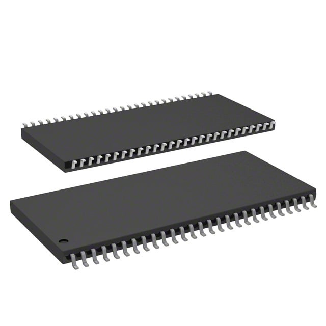
IS42S16160B-7TI
| Part Description |
IC DRAM 256MBIT PAR 54TSOP II |
|---|---|
| Quantity | 480 Available (as of June 15, 2026) |

| Product Category | Memory |
|---|---|
| Manufacturer | Integrated Silicon Solution Inc |
| Manufacturing Status | Obsolete |
| Manufacturer Standard Lead Time | Contact Us |
| Datasheet |
Specifications & Environmental
| Device Package | 54-TSOP II | Memory Format | DRAM | Technology | SDRAM | ||
|---|---|---|---|---|---|---|---|
| Memory Size | 256 Mbit | Access Time | 5.4 ns | Grade | Industrial | ||
| Clock Frequency | 143 MHz | Voltage | 3V ~ 3.6V | Memory Type | Volatile | ||
| Operating Temperature | -40°C ~ 85°C (TA) | Write Cycle Time Word Page | N/A | Packaging | 54-TSOP (0.400", 10.16mm Width) | ||
| Mounting Method | Volatile | Memory Interface | Parallel | Memory Organization | 16M x 16 | ||
| Moisture Sensitivity Level | 3 (168 Hours) | RoHS Compliance | ROHS3 Compliant | REACH Compliance | REACH Unaffected | ||
| Qualification | N/A | ECCN | EAR99 | HTS Code | 8542.32.0024 |
Overview of IS42S16160B-7TI – IC DRAM 256MBIT PAR 54TSOP II
The IS42S16160B-7TI is a 256‑Mbit synchronous DRAM organized as 16M × 16 with a parallel LVTTL interface and quad‑bank internal architecture. It implements a pipeline synchronous design with programmable burst and CAS timing to support high‑rate, burst‑oriented memory transfers.
Designed for 3.0–3.6 V systems (3.3 V operation per device specification) and rated for -40°C to 85°C, the device targets systems that require a compact 54‑pin TSOP‑II (10.16 mm) footprint and deterministic SDRAM behavior for buffering and high‑speed data access.
Key Features
- Memory Architecture — 256 Mbit SDRAM organized as 16M × 16 with quad internal banks to support interleaved access and hidden row precharge.
- Performance — Supports clock frequencies of 166, 143, and 133 MHz (‑6, ‑7, ‑8 timing options) with programmable CAS latency of 2 or 3 and access time from clock as low as 5.4 ns (CAS = 3).
- Burst and Sequencing — Programmable burst lengths (1, 2, 4, 8, full page) and selectable sequential or interleave burst sequencing for flexible data transfer patterns.
- Refresh and Power Modes — Auto Refresh, Self Refresh and CBR features with 8K refresh cycles every 64 ms for data retention and power management.
- Interface and Signaling — LVTTL‑compatible inputs/outputs and parallel memory interface suitable for synchronous, clock‑edge referenced operation.
- Voltage and Supply — Operates across a 3.0 V to 3.6 V supply range; designed for 3.3 V memory systems per device specification.
- Package and Temperature — Available in 54‑pin TSOP‑II (0.400", 10.16 mm width) and specified for industrial temperature operation from -40°C to 85°C.
Typical Applications
- Industrial systems — Memory buffering and data storage in systems that require operation across an industrial temperature range (-40°C to 85°C).
- Parallel data subsystems — 16‑bit parallel memory expansion where a 16M × 16 organization and LVTTL interface are required for burst transfers and deterministic timing.
- High‑rate buffering — Synchronous burst read/write operations for designs that leverage programmable burst lengths and CAS latency to tune throughput and latency.
Unique Advantages
- Configurable performance — Programmable CAS latency (2 or 3) and multiple clock grades (166/143/133 MHz) let designers match timing to system requirements.
- Flexible burst modes — Burst lengths from 1 to full page and selectable sequential/interleave sequencing simplify data transfer patterns and reduce controller complexity.
- Quad‑bank architecture — Internal bank structure supports bank interleaving to hide precharge time and improve sustained access efficiency.
- Industrial temperature rating — Specified operation from -40°C to 85°C addresses thermal requirements for deployed industrial electronics.
- Space‑efficient package — 54‑pin TSOP‑II (10.16 mm width) delivers a compact footprint for board designs with parallel SDRAM needs.
Why Choose IS42S16160B-7TI?
The IS42S16160B-7TI provides a deterministic, synchronous 256‑Mbit DRAM solution with programmable timing, burst flexibility, and an internal quad‑bank architecture that supports efficient high‑rate transfers. Its 16M × 16 organization and LVTTL interface make it a direct fit for designs requiring parallel SDRAM in a compact TSOP‑II package.
This device is suitable for engineers and procurement teams specifying memory for systems operating at standard 3.3 V memory voltages and across industrial temperature ranges, offering tunable performance and established SDRAM control features such as auto/self refresh and burst termination mechanisms.
Request a quote or submit an inquiry to obtain pricing, availability, or technical assistance for the IS42S16160B-7TI.