IS42S16160B-7TLI
| Part Description |
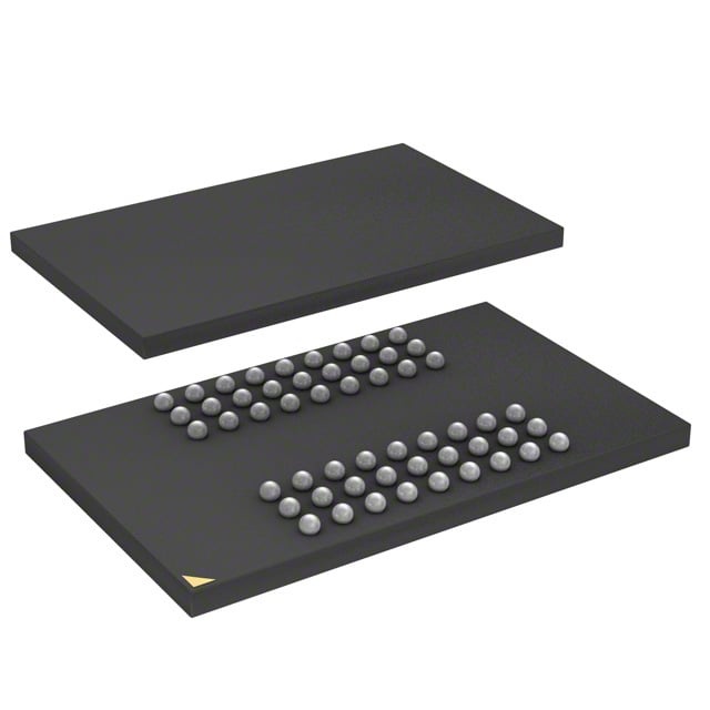
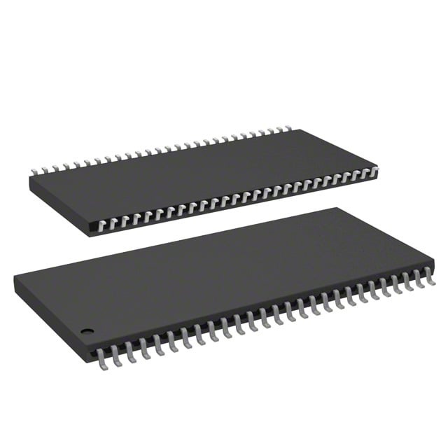
IC DRAM 256MBIT PAR 54TSOP II |
|---|---|
| Quantity | 1,702 Available (as of June 15, 2026) |

| Product Category | Memory |
|---|---|
| Manufacturer | Integrated Silicon Solution Inc |
| Manufacturing Status | Obsolete |
| Manufacturer Standard Lead Time | Contact Us |
| Datasheet |
Specifications & Environmental
| Device Package | 54-TSOP II | Memory Format | DRAM | Technology | SDRAM | ||
|---|---|---|---|---|---|---|---|
| Memory Size | 256 Mbit | Access Time | 5.4 ns | Grade | Industrial | ||
| Clock Frequency | 143 MHz | Voltage | 3V ~ 3.6V | Memory Type | Volatile | ||
| Operating Temperature | -40°C ~ 85°C (TA) | Write Cycle Time Word Page | N/A | Packaging | 54-TSOP (0.400", 10.16mm Width) | ||
| Mounting Method | Volatile | Memory Interface | Parallel | Memory Organization | 16M x 16 | ||
| Moisture Sensitivity Level | 3 (168 Hours) | RoHS Compliance | ROHS3 Compliant | REACH Compliance | REACH Unaffected | ||
| Qualification | N/A | ECCN | EAR99 | HTS Code | 8542.32.0024 |
Overview of IS42S16160B-7TLI – IC DRAM 256MBIT PAR 54TSOP II
The IS42S16160B-7TLI is a 256 Mbit synchronous DRAM organized as 16M × 16 with a parallel memory interface and a 54-pin TSOP-II package. It implements a fully synchronous, quad-bank architecture with pipeline operation to support high-speed, burst-oriented data transfers in 3.3 V memory systems.
Designed for systems that require deterministic, high-throughput memory operations, this device offers programmable burst lengths and CAS latency options, power-saving refresh modes, and an industrial operating temperature range for use in temperature-constrained applications.
Key Features
- Memory Architecture 256 Mbit SDRAM organized as 16M × 16 with internal quad-bank configuration to support concurrent bank operations and hidden row precharge.
- Performance Clock rate up to 143 MHz (‑7 speed grade) with an access time from clock of 5.4 ns (CAS latency = 3), and programmable CAS latency of 2 or 3 clocks for performance tuning.
- Burst and Access Modes Programmable burst length (1, 2, 4, 8, full page) and burst sequence (sequential/interleave), supporting burst read/write and burst read/single write operations with burst termination options.
- Refresh and Power Management Auto Refresh and Self Refresh support with 8K refresh cycles every 64 ms, plus a power-down mode to reduce standby power.
- Interface Fully synchronous operation with all signals referenced to the positive clock edge and LVTTL-compatible inputs/outputs for standard 3.3 V memory system integration.
- Voltage and Temperature Operating supply range of 3.0 V to 3.6 V and an industrial operating temperature range of -40 °C to 85 °C.
- Package 54-pin TSOP-II (0.400", 10.16 mm width) package; the device family is also offered in 54-ball BGA (x16 only) and available in lead-free options.
Typical Applications
- 3.3 V Memory Subsystems Used as synchronous DRAM memory in 3.3 V system architectures where deterministic burst transfers and CAS latency control are required.
- Embedded Systems Provides 256 Mbit of volatile storage for embedded controllers and processors that require pipelined, high-speed parallel memory access.
- Industrial Equipment Suitable for industrial designs that need extended temperature operation (‑40 °C to 85 °C) while maintaining SDRAM performance.
Unique Advantages
- Synchronous Pipeline Architecture: Registered inputs and outputs referenced to the clock edge enable predictable, high-speed burst transfers.
- Flexible Performance Tuning: Programmable CAS latency and selectable burst lengths/sequence allow designers to match memory timing to system requirements.
- Bank Interleaving and Hidden Precharge: Internal multi-bank design hides row-access/precharge time to improve effective throughput in random-access patterns.
- Power-saving Modes: Auto Refresh, Self Refresh and power-down reduce standby power in duty-cycled or low-activity systems.
- Industrial-grade Operating Range: Wide operating temperature and standard 3.0–3.6 V supply compatibility simplify integration into industrial and harsh-environment designs.
- Standard Packaging Options: 54-pin TSOP-II package provides a compact, board-level solution with lead-free availability for manufacturing flexibility.
Why Choose IS42S16160B-7TLI?
The IS42S16160B-7TLI positions itself as a deterministic, high-speed SDRAM option for designs that demand programmable burst behavior, selectable CAS latency, and robust refresh/power modes. Its 16M × 16 organization and quad-bank architecture deliver the memory density and internal concurrency needed for sustained burst transfers in 3.3 V systems.
This device is well suited for engineers specifying memory for embedded and industrial applications where extended temperature range, predictable timing (5.4 ns access time @ CL=3), and standard TSOP-II packaging are required. The combination of configurable timing, bank interleaving, and refresh capabilities provides long-term design flexibility and operational reliability.
Request a quote or submit a pricing and availability inquiry to discuss lead times, package options, and volume pricing for the IS42S16160B-7TLI.