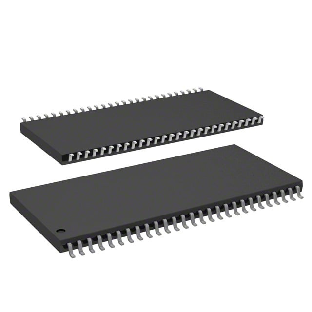
IS42S16160B-7TL-TR
| Part Description |
IC DRAM 256MBIT PAR 54TSOP II |
|---|---|
| Quantity | 188 Available (as of June 14, 2026) |

| Product Category | Memory |
|---|---|
| Manufacturer | Integrated Silicon Solution Inc |
| Manufacturing Status | Obsolete |
| Manufacturer Standard Lead Time | Contact Us |
| Datasheet |
Specifications & Environmental
| Device Package | 54-TSOP II | Memory Format | DRAM | Technology | SDRAM | ||
|---|---|---|---|---|---|---|---|
| Memory Size | 256 Mbit | Access Time | 5.4 ns | Grade | Commercial | ||
| Clock Frequency | 143 MHz | Voltage | 3V ~ 3.6V | Memory Type | Volatile | ||
| Operating Temperature | 0°C ~ 70°C (TA) | Write Cycle Time Word Page | N/A | Packaging | 54-TSOP (0.400", 10.16mm Width) | ||
| Mounting Method | Volatile | Memory Interface | Parallel | Memory Organization | 16M x 16 | ||
| Moisture Sensitivity Level | 3 (168 Hours) | RoHS Compliance | ROHS3 Compliant | REACH Compliance | REACH Unaffected | ||
| Qualification | N/A | ECCN | EAR99 | HTS Code | 8542.32.0024 |
Overview of IS42S16160B-7TL-TR – IC DRAM 256MBIT PAR 54TSOP II
The IS42S16160B-7TL-TR is a 256 Mbit synchronous DRAM (SDRAM) organized as 16M × 16 with a parallel memory interface and quad-bank architecture. It uses a pipelined, fully synchronous design with all signals referenced to the rising edge of the clock for predictable, high-speed burst transfers.
Targeted for designs requiring medium-density, fast, volatile memory, this device delivers 143 MHz clock operation (CL=3) with programmable burst length and sequence, making it suitable for systems that need deterministic, high-throughput DRAM behavior within a 0°C to 70°C operating range.
Key Features
- Memory Type & Organization — 256 Mbit SDRAM, organized as 16M × 16 with four internal banks (4M × 16 × 4 banks) for bank interleaving and hidden precharge.
- Clock & Timing — Rated for 143 MHz operation at CAS Latency = 3 (-7 speed grade) with an access time from clock of 5.4 ns (CL=3).
- Programmable Burst & CAS — Supports programmable burst lengths (1, 2, 4, 8, full page) and programmable burst sequence (Sequential/Interleave); CAS latency programmable between 2 and 3 clocks.
- Refresh & Power Modes — Auto Refresh and Self Refresh supported; 8K refresh cycles every 64 ms per datasheet specification to maintain data integrity in self-refresh.
- Interface & Logic Levels — LVTTL-compatible I/O with a parallel memory interface for conventional SDRAM system integration.
- Power Supply — Specified supply range 3.0 V to 3.6 V; datasheet references 3.3 V VDD and 3.3 V VDDQ operation.
- Package — Available in 54-pin TSOP II (0.400", 10.16 mm width) package suitable for surface-mount designs.
- Operating Temperature — Commercial grade operating range of 0°C to 70°C; datasheet also notes availability in industrial temperature variants.
Typical Applications
- System Memory for Embedded Platforms — 256 Mbit density and 143 MHz synchronous operation provide deterministic burst transfers for embedded controllers and processors that require parallel SDRAM.
- Frame Buffering & Data Buffering — Quad-bank architecture and programmable burst lengths support burst-oriented read/write sequences for buffering tasks that need high throughput.
- General-Purpose DRAM Expansion — Parallel interface and LVTTL signaling allow integration into legacy and modern boards requiring a standard SDRAM memory block.
Unique Advantages
- Deterministic Synchronous Operation: Fully synchronous design with clock-referenced I/O ensures predictable timing for burst access patterns.
- Configurable Performance: Programmable CAS latency (2 or 3 clocks) and multiple burst lengths let designers tune latency and throughput to system needs.
- Bank Interleaving: Four internal banks and internal precharge hide row access/precharge cycles, improving effective throughput for random accesses.
- Standard Power Supply: Operates within a common 3.0–3.6 V supply window (datasheet references 3.3 V), simplifying power-rail integration in existing systems.
- Compact Surface-Mount Packaging: 54-pin TSOP II package (0.400", 10.16 mm width) supports high-density PCB layouts while providing a conventional footprint for SDRAM.
Why Choose IS42S16160B-7TL-TR?
The IS42S16160B-7TL-TR combines a 256 Mbit SDRAM density with a fully synchronous, quad-bank architecture and programmable timing to deliver flexible, predictable memory behavior for embedded and system-level applications. Its 143 MHz (-7) performance point with a 5.4 ns access time (CL=3) is suited to designs that require controlled latency and burst transfer capability.
This part is appropriate for designers seeking a standard parallel SDRAM solution in a 54-pin TSOP II package, offering configurable burst modes, LVTTL compatibility, and standard 3.0–3.6 V power requirements. The device’s refresh and self-refresh support, along with bank interleaving, provide practical benefits for buffering and memory expansion in compact board designs.
If you would like pricing, availability, or technical packaging details for IS42S16160B-7TL-TR, request a quote or contact sales for additional information and ordering support.