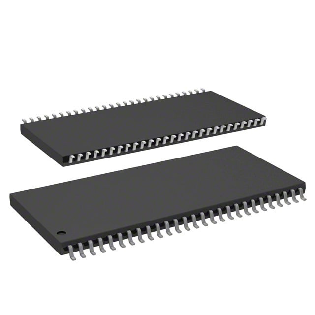
IS42S16160B-7TL
| Part Description |
IC DRAM 256MBIT PAR 54TSOP II |
|---|---|
| Quantity | 387 Available (as of June 15, 2026) |

| Product Category | Memory |
|---|---|
| Manufacturer | Integrated Silicon Solution Inc |
| Manufacturing Status | Obsolete |
| Manufacturer Standard Lead Time | Contact Us |
| Datasheet |
Specifications & Environmental
| Device Package | 54-TSOP II | Memory Format | DRAM | Technology | SDRAM | ||
|---|---|---|---|---|---|---|---|
| Memory Size | 256 Mbit | Access Time | 5.4 ns | Grade | Commercial | ||
| Clock Frequency | 143 MHz | Voltage | 3V ~ 3.6V | Memory Type | Volatile | ||
| Operating Temperature | 0°C ~ 70°C (TA) | Write Cycle Time Word Page | N/A | Packaging | 54-TSOP (0.400", 10.16mm Width) | ||
| Mounting Method | Volatile | Memory Interface | Parallel | Memory Organization | 16M x 16 | ||
| Moisture Sensitivity Level | 3 (168 Hours) | RoHS Compliance | ROHS3 Compliant | REACH Compliance | REACH Unaffected | ||
| Qualification | N/A | ECCN | EAR99 | HTS Code | 8542.32.0024 |
Overview of IS42S16160B-7TL – IC DRAM 256MBIT PAR 54TSOP II
The IS42S16160B-7TL is a 256‑Mbit synchronous DRAM organized as 16M × 16 with a parallel memory interface. It implements a fully synchronous, quad‑bank architecture with pipeline operation and LVTTL‑compatible signaling referenced to the positive clock edge.
This device targets designs requiring a 256‑Mbit parallel SDRAM solution with programmable burst control, selectable CAS latency, and standard 54‑pin TSOP‑II packaging, operating from 3.0 V to 3.6 V and within a 0 °C to 70 °C ambient range.
Key Features
- Memory Type & Architecture 256‑Mbit SDRAM, organized as 16M × 16 with quad internal banks for interleaved access and hidden row precharge.
- Performance Supports clock frequencies up to 143 MHz for the -7 speed grade with access time from clock as low as 5.4 ns (CAS latency = 3).
- Programmable Burst & CAS Programmable burst lengths (1, 2, 4, 8, full page) and selectable burst sequence (sequential/interleave); CAS latency programmable to 2 or 3 clocks.
- Refresh & Power Modes Auto Refresh and Self Refresh support with 8K refresh cycles every 64 ms; includes power‑down mode and auto precharge options.
- Interface & Signaling LVTTL compatible inputs/outputs; all signals are registered on the rising edge of CLK for fully synchronous operation.
- Supply Voltage Operates from 3.0 V to 3.6 V with 3.3 V nominal VDD and VDDQ per device specification.
- Package & Mounting 54‑pin TSOP‑II (0.400", 10.16 mm width) package; supplier device package listed as 54‑TSOP II.
- Temperature Range Commercial ambient operating range: 0 °C to 70 °C.
- Availability Options Device is available in lead‑free variants and in alternate package options (54‑ball BGA noted in device family documentation).
Typical Applications
- High‑speed data buffering Used where burst read/write operations and random column access every clock cycle benefit throughput and latency.
- System memory for parallel SDRAM interfaces Fits designs requiring a 256‑Mbit parallel SDRAM with LVTTL signaling and selectable CAS latency.
- Memory subsystems with refresh and low‑power needs Auto and self‑refresh modes reduce management overhead in power‑sensitive designs.
Unique Advantages
- Synchronous pipeline architecture: All I/O is referenced to the positive clock edge, enabling predictable, high‑speed burst transfers.
- Flexible burst control: Programmable burst lengths and sequential/interleave sequencing allow designers to match memory behavior to system access patterns.
- Selectable CAS latency: CAS = 2 or 3 options provide tradeoffs between clock frequency and access timing for system optimization.
- Integrated refresh management: Auto and self refresh with defined 8K/64 ms refresh handling simplify system refresh requirements.
- Standard TSOP‑II package: 54‑pin TSOP‑II (10.16 mm width) supports compact board layouts while maintaining parallel x16 data bus connectivity.
- Commercial temperature and 3.3 V operation: Matches common system power rails and operating environments for mainstream embedded applications.
Why Choose IC DRAM 256MBIT PAR 54TSOP II?
The IS42S16160B-7TL delivers a straightforward, fully synchronous 256‑Mbit SDRAM solution for systems that require predictable, burst‑oriented memory performance and a parallel x16 data interface. Its programmable burst options, selectable CAS latency, and internal bank architecture provide designers with flexibility to tune throughput and latency to application needs.
This device is well suited to designers seeking a 3.3 V nominal SDRAM in a compact 54‑pin TSOP‑II package with built‑in refresh and low‑power modes. The combination of timing options, synchronous signaling, and available lead‑free variants supports robust integration into a range of commercial electronic systems.
Request a quote or submit a sales inquiry to obtain availability, pricing, and lead‑time information for the IS42S16160B-7TL.