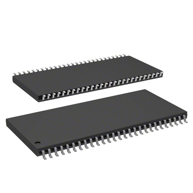
IS42S16400F-7TLI
| Part Description |
IC DRAM 64MBIT PAR 54TSOP II |
|---|---|
| Quantity | 753 Available (as of June 10, 2026) |

| Product Category | Memory |
|---|---|
| Manufacturer | Integrated Silicon Solution Inc |
| Manufacturing Status | Obsolete |
| Manufacturer Standard Lead Time | Contact Us |
| Datasheet |
Specifications & Environmental
| Device Package | 54-TSOP II | Memory Format | DRAM | Technology | SDRAM | ||
|---|---|---|---|---|---|---|---|
| Memory Size | 64 Mbit | Access Time | 5.4 ns | Grade | Industrial | ||
| Clock Frequency | 143 MHz | Voltage | 3V ~ 3.6V | Memory Type | Volatile | ||
| Operating Temperature | -40°C ~ 85°C (TA) | Write Cycle Time Word Page | N/A | Packaging | 54-TSOP (0.400", 10.16mm Width) | ||
| Mounting Method | Volatile | Memory Interface | Parallel | Memory Organization | 4M x 16 | ||
| Moisture Sensitivity Level | 3 (168 Hours) | RoHS Compliance | ROHS3 Compliant | REACH Compliance | REACH Unaffected | ||
| Qualification | N/A | ECCN | EAR99 | HTS Code | 8542.32.0002 |
Overview of IS42S16400F-7TLI – IC DRAM 64MBIT PAR 54TSOP II
The IS42S16400F-7TLI is a 64 Mbit synchronous DRAM organized as 1,048,576 × 16 × 4 banks. It implements a pipeline, fully synchronous architecture with all signals referenced to the rising edge of the clock to support high-speed parallel memory operations.
Designed for systems requiring fast parallel SDRAM with flexible burst and timing options, this device offers industry-grade operating temperature range and a compact 54-pin TSOP II package for space-constrained applications.
Key Features
- Core / Memory Organization 64 Mbit density organized as 4M × 16 with 4 internal banks to improve throughput and hide row access/precharge latency.
- Timing & Performance Supports clock frequencies up to 143 MHz for the -7 speed grade with CAS latency options (2 or 3 clocks) and an access time from clock of 5.4 ns at CL=3.
- Programmable Burst & Sequence Programmable burst length (1, 2, 4, 8, full page) and selectable sequential or interleave burst sequences for flexible data transfer patterns.
- Refresh & Retention Auto refresh (CBR) and self-refresh modes supported; 4096 refresh cycles per 64 ms for commercial/industrial/A1 grades (A2 grade uses 16 ms).
- Interface & Logic Levels LVTTL-compatible interface with fully synchronous control referenced to a single positive-edge clock input.
- Power Single 3.3 V supply range (3.0 V to 3.6 V) for standard SDRAM system integration.
- Package & Temperature 54-pin TSOP II package (0.400", 10.16 mm width) and an operating temperature range of -40°C to +85°C (TA) for industrial applications.
Typical Applications
- Industrial Systems The -40°C to +85°C operating range and parallel SDRAM interface make it suitable for industrial control and embedded applications that require reliable memory at extended temperatures.
- Embedded Memory Expansion Provides a compact, high-speed parallel memory option for embedded designs needing 64 Mbit SDRAM capacity and flexible burst operation.
- High‑Speed Data Buffering The 4-bank architecture and programmable burst modes support applications that require predictable, high-throughput buffering and burst transfers.
Unique Advantages
- Flexible Timing Options: Programmable CAS latency (2 or 3 clocks) and selectable burst lengths let designers tune latency and throughput to match system timing.
- Single 3.3 V Supply: Standard 3.0–3.6 V supply simplifies power rails and integration with common system logic levels.
- Compact TSOP II Package: 54-pin TSOP II (10.16 mm width) delivers a small footprint for space-sensitive board designs.
- Built‑in Refresh Management: Auto refresh and self-refresh modes with defined refresh cycles reduce system refresh overhead and support low-power retention scenarios.
- Deterministic Synchronous Operation: Fully synchronous design with LVTTL interface and positive-edge clock reference supports predictable, pipelined memory transfers.
- Industrial Temperature Rating: Operation from -40°C to +85°C (TA) addresses a broad range of non-automotive industrial environments.
Why Choose IS42S16400F-7TLI?
The IS42S16400F-7TLI combines a 64 Mbit density with a fully synchronous, pipelined SDRAM architecture and flexible programmability for burst length and CAS latency. Its single 3.3 V supply, LVTTL interface, and 4-bank organization provide a balance of performance and integration for parallel-memory designs that require predictable timing and high-throughput buffering.
This device is particularly well suited to designers targeting industrial-grade embedded systems and compact boards that need a reliable, documented SDRAM solution with configurable timing and refresh behavior.
Request a quote or submit an inquiry for pricing and availability to initiate evaluation and procurement.