IS42S16400F-7TL
| Part Description |
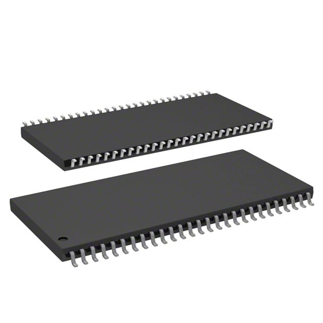
IC DRAM 64MBIT PAR 54TSOP II |
|---|---|
| Quantity | 11 Available (as of June 15, 2026) |

| Product Category | Memory |
|---|---|
| Manufacturer | Integrated Silicon Solution Inc |
| Manufacturing Status | Obsolete |
| Manufacturer Standard Lead Time | Contact Us |
| Datasheet |
Specifications & Environmental
| Device Package | 54-TSOP II | Memory Format | DRAM | Technology | SDRAM | ||
|---|---|---|---|---|---|---|---|
| Memory Size | 64 Mbit | Access Time | 5.4 ns | Grade | Commercial | ||
| Clock Frequency | 143 MHz | Voltage | 3V ~ 3.6V | Memory Type | Volatile | ||
| Operating Temperature | 0°C ~ 70°C (TA) | Write Cycle Time Word Page | N/A | Packaging | 54-TSOP (0.400", 10.16mm Width) | ||
| Mounting Method | Volatile | Memory Interface | Parallel | Memory Organization | 4M x 16 | ||
| Moisture Sensitivity Level | 3 (168 Hours) | RoHS Compliance | ROHS3 Compliant | REACH Compliance | REACH Unaffected | ||
| Qualification | N/A | ECCN | EAR99 | HTS Code | 8542.32.0002 |
Overview of IS42S16400F-7TL – IC DRAM 64MBIT PAR 54TSOP II
The IS42S16400F-7TL is a 64‑Mbit synchronous DRAM (SDRAM) organized as 1,048,576 × 16 × 4 banks, implementing pipeline architecture for high‑speed synchronous data transfer. It is a fully synchronous, parallel memory device with LVTTL signaling designed for commercial temperature applications.
This device targets system designs that require transient, high‑speed volatile memory with programmable burst modes, internal bank management, and standard 54‑pin TSOP II packaging. The -7 speed grade supports a clock frequency of 143 MHz and an access time from clock of 5.4 ns (CAS latency = 3).
Key Features
- Memory Core — 64 Mbit SDRAM organized as 4M × 16 (1M × 16 × 4 banks) for parallel data access and internal banked operation.
- High‑Speed Synchronous Operation — Fully synchronous operation with all signals referenced to the rising edge of the clock; -7 speed grade supports 143 MHz clock and 5.4 ns access time (CAS latency = 3).
- Burst and Access Modes — Programmable burst length (1, 2, 4, 8, full page) and programmable burst sequence (sequential/interleave); supports burst read/write and burst read/single write operations with burst termination commands.
- Latency and Timing — Programmable CAS latency options of 2 or 3 clocks to match system timing requirements.
- Refresh and Power Modes — Auto refresh (CBR) and self‑refresh modes; standard refresh count of 4K cycles per 64 ms for commercial/industrial grades as specified.
- Interface and Supply — LVTTL-compatible interface with a single 3.3 V power supply; specified operating voltage range 3.0 V to 3.6 V.
- Package and Mounting — 54‑pin TSOP II (0.400", 10.16 mm width) surface‑mount package for compact board-level integration.
- Operating Range — Commercial temperature range specified as 0 °C to 70 °C (TA).
Typical Applications
- High‑speed buffer memory — Use as transient system memory where synchronous, low‑latency burst transfers are required.
- System memory for commercial electronics — Suitable for designs operating in the 0 °C to 70 °C range that require a 3.3 V supply and standard TSOP II packaging.
- Temporary data storage — Ideal for applications that rely on programmable burst lengths and internal bank management for efficient data handling.
Unique Advantages
- Banked architecture for hidden row access — Internal 4‑bank organization reduces row access/precharge latency by allowing concurrent bank operations.
- Flexible burst control — Programmable burst lengths and sequences enable optimized throughput and predictable data streaming behavior.
- Configurable latency — CAS latency options (2 or 3 clocks) allow designers to tune timing for target system clock rates.
- Standard supply and interface — Single 3.3 V supply and LVTTL signaling simplify power and interface design in commercial systems.
- Compact TSOP II package — 54‑pin TSOP II package supports high‑density board layouts while maintaining accessible pinout for parallel memory interfaces.
Why Choose IS42S16400F-7TL?
The IS42S16400F-7TL delivers a verified synchronous DRAM solution with a 4‑bank, 16‑bit data organization and programmable burst and latency options to match a range of commercial system timing needs. Its pipeline architecture and LVTTL interface enable predictable, clock‑referenced operation at the -7 speed grade (143 MHz), while the 54‑pin TSOP II package supports compact integration.
This device is well suited to designers needing a 64‑Mbit volatile memory component for commercial temperature applications where standard 3.3 V supply operation, flexible burst behavior, and low access latency are important design drivers.
Request a quote or contact sales to discuss availability, pricing, and technical support for IS42S16400F-7TL.