IS42S16400F-7BLI
| Part Description |
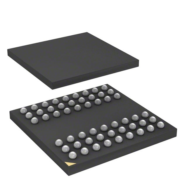
IC DRAM 64MBIT PAR 54TFBGA |
|---|---|
| Quantity | 230 Available (as of June 14, 2026) |

| Product Category | Memory |
|---|---|
| Manufacturer | Integrated Silicon Solution Inc |
| Manufacturing Status | Obsolete |
| Manufacturer Standard Lead Time | Contact Us |
| Datasheet |
Specifications & Environmental
| Device Package | 54-TFBGA (8x8) | Memory Format | DRAM | Technology | SDRAM | ||
|---|---|---|---|---|---|---|---|
| Memory Size | 64 Mbit | Access Time | 5.4 ns | Grade | Industrial | ||
| Clock Frequency | 143 MHz | Voltage | 3V ~ 3.6V | Memory Type | Volatile | ||
| Operating Temperature | -40°C ~ 85°C (TA) | Write Cycle Time Word Page | N/A | Packaging | 54-TFBGA | ||
| Mounting Method | Volatile | Memory Interface | Parallel | Memory Organization | 4M x 16 | ||
| Moisture Sensitivity Level | 3 (168 Hours) | RoHS Compliance | ROHS3 Compliant | REACH Compliance | REACH Unaffected | ||
| Qualification | N/A | ECCN | EAR99 | HTS Code | 8542.32.0002 |
Overview of IS42S16400F-7BLI – IC DRAM 64MBIT PAR 54TFBGA
The IS42S16400F-7BLI is a 64 Mbit synchronous DRAM (SDRAM) organized as 1,048,576 × 16 × 4 banks. It implements a pipelined, fully synchronous architecture with all signals referenced to the rising clock edge, providing predictable timing for parallel memory systems.
Designed for commercial and industrial designs, this device offers programmable burst lengths and CAS latency options, single 3.3 V supply operation, and a compact 54-ball TFBGA (8 mm × 8 mm) package to balance performance and board space.
Key Features
- Memory Organization — 64 Mbit configured as 4M × 16 with 4 internal banks for improved internal access and precharge management.
- Synchronous SDRAM Core — Fully synchronous operation with pipeline architecture; all inputs and outputs referenced to the rising clock edge.
- Performance Options — Clock frequency option for the -7 variant is 143 MHz with an access time from clock of 5.4 ns (CAS latency = 3).
- Programmable Operation — Supports programmable burst lengths (1, 2, 4, 8, full page) and programmable burst sequence (sequential/interleave), plus CAS latency selectable between 2 and 3 clocks.
- Refresh and Power Management — Auto refresh (CBR) and self-refresh modes with 4096 refresh cycles per 64 ms (commercial/industrial options) to maintain data integrity during idle periods.
- Interface and Signaling — Parallel memory interface with LVTTL signaling for control inputs.
- Voltage and Temperature — Single-supply operation across 3.0 V to 3.6 V and rated operating temperature range of −40 °C to +85 °C (TA) for industrial use.
- Package — 54-ball TFBGA (8 mm × 8 mm) surface-mount package for compact board integration.
Typical Applications
- Industrial Control Systems — Provides synchronous parallel memory with industrial temperature range (−40 °C to +85 °C) for embedded controllers and PLCs.
- Embedded Systems — 64 Mbit capacity and programmable burst/CAS behavior suit embedded designs that require deterministic, high-speed parallel DRAM.
- Commercial Electronics — Commercial-temperature options and a compact 54-TFBGA package enable integration into consumer and commercial products where board space is limited.
Unique Advantages
- Configurable Performance: Programmable CAS latency (2 or 3) and multiple burst length/sequence options let designers tune throughput and latency for target workloads.
- Predictable Timing: Fully synchronous, pipelined architecture and specified access times (5.4 ns for the -7 part at CAS = 3) support deterministic memory timing in parallel systems.
- Compact Package: 54-ball TFBGA (8×8 mm) enables high-density board layouts while retaining a parallel SDRAM interface.
- Robust Refresh Support: Auto and self-refresh modes with defined refresh cycles ensure data retention during idle or low-power intervals.
- Wide Voltage and Temperature Range: 3.0–3.6 V supply tolerance and −40 °C to +85 °C operating range accommodate diverse commercial and industrial environments.
- Banked Memory Architecture: Four internal banks help hide row access/precharge latency and improve effective throughput for burst accesses.
Why Choose IC DRAM 64MBIT PAR 54TFBGA?
The IS42S16400F-7BLI delivers a balanced combination of capacity, configurable performance and compact packaging for designs that require synchronous parallel DRAM. Its banked architecture, programmable burst behavior and selectable CAS latency provide engineers the control needed to optimize throughput and latency for system-level requirements.
This device is well suited to commercial and industrial applications where a 64 Mbit SDRAM with 3.3 V operation, defined timing characteristics, and a small 54-ball TFBGA footprint are required. The included refresh management and LVTTL interface simplify integration into existing memory subsystems while maintaining predictable timing behavior.
Request a quote or submit a product inquiry to receive pricing, lead-time information, and technical support for the IS42S16400F-7BLI.