IS42S16400F-7BL
| Part Description |
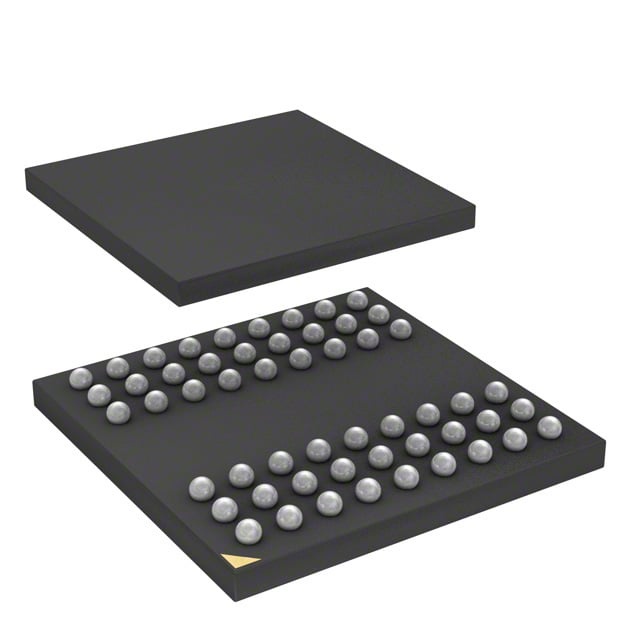
IC DRAM 64MBIT PAR 54TFBGA |
|---|---|
| Quantity | 489 Available (as of June 9, 2026) |

| Product Category | Memory |
|---|---|
| Manufacturer | Integrated Silicon Solution Inc |
| Manufacturing Status | Obsolete |
| Manufacturer Standard Lead Time | Contact Us |
| Datasheet |
Specifications & Environmental
| Device Package | 54-TFBGA (8x8) | Memory Format | DRAM | Technology | SDRAM | ||
|---|---|---|---|---|---|---|---|
| Memory Size | 64 Mbit | Access Time | 5.4 ns | Grade | Commercial | ||
| Clock Frequency | 143 MHz | Voltage | 3V ~ 3.6V | Memory Type | Volatile | ||
| Operating Temperature | 0°C ~ 70°C (TA) | Write Cycle Time Word Page | N/A | Packaging | 54-TFBGA | ||
| Mounting Method | Volatile | Memory Interface | Parallel | Memory Organization | 4M x 16 | ||
| Moisture Sensitivity Level | 3 (168 Hours) | RoHS Compliance | ROHS3 Compliant | REACH Compliance | REACH Unaffected | ||
| Qualification | N/A | ECCN | EAR99 | HTS Code | 8542.32.0002 |
Overview of IS42S16400F-7BL – IC DRAM 64MBIT PAR 54TFBGA
The IS42S16400F-7BL is a 64‑Mbit synchronous DRAM organized as 1,048,576 × 16 × 4 banks, delivering pipelined, high‑speed parallel memory for synchronous designs. It implements internal banking and a fully synchronous interface referenced to the rising clock edge to support predictable, high‑throughput memory transactions.
This device targets systems that require a compact 64‑Mbit SDRAM in a 54‑ball TFBGA (8mm × 8mm) package, offering programmable burst and timing options plus standard 3.3V single‑supply operation for integration into parallel memory subsystems.
Key Features
- Memory Organization: 64 Mbit organized as 1,048,576 × 16 × 4 banks for improved concurrency and throughput.
- Synchronous SDRAM Core: Fully synchronous operation with all signals referenced to the positive clock edge and pipelined architecture for high‑speed data transfer.
- Clock and Timing Options: Supports clock frequencies including 143 MHz (‑7 speed grade) with programmable CAS latency of 2 or 3 clocks and access time as low as 5.4 ns (CL = 3, ‑7).
- Burst and Sequencing: Programmable burst lengths (1, 2, 4, 8, full page) and burst sequence selectable between Sequential and Interleave; supports burst read/write and burst read/single write modes with burst termination commands.
- Refresh and Retention: Auto refresh (CBR) and self‑refresh modes supported; 4,096 refresh cycles every 64 ms for Commercial/Industrial/A1 grades or 16 ms for A2 grade as specified in the device options.
- Interface and Signaling: LVTTL interface for control and data signaling; random column address capability every clock cycle.
- Power: Single 3.3 V power supply operation with an allowed supply range of 3.0 V to 3.6 V.
- Package and Temperature: 54‑ball TFBGA (8 mm × 8 mm) package; commercial operating temperature range 0 °C to +70 °C (TA).
Unique Advantages
- Flexible timing and performance: Multiple speed grades and programmable CAS latency let designers balance access time and clock frequency to meet system timing targets.
- Banked architecture for concurrency: Four internal banks and internal precharge/bank‑hiding improve effective throughput on interleaved access patterns.
- Programmable burst behavior: Choice of burst lengths and sequence modes simplifies interface design for different data transfer patterns and system memory controllers.
- Standard single‑supply integration: 3.3 V single supply (3.0–3.6 V range) and LVTTL signaling ease integration with common legacy and embedded systems.
- Compact BGA footprint: 54‑TFBGA (8×8 mm) package provides a small board footprint for dense system designs while retaining a parallel memory interface.
Why Choose IC DRAM 64MBIT PAR 54TFBGA?
The IS42S16400F‑7BL delivers a straightforward, synchronous 64‑Mbit DRAM solution with configurable burst and timing features, internal banking for improved concurrency, and a compact 54‑ball TFBGA footprint. Its programmable CAS latency and multiple clock frequency grades provide design flexibility for a range of parallel memory implementations.
This device is suited for designs requiring a standard 64‑Mbit SDRAM with predictable synchronous timing, refresh management, and a common 3.3 V supply. The combination of banked architecture, burst configurability, and compact packaging supports efficient board integration and predictable performance across supported operating conditions.
Request a quote or submit an inquiry to receive pricing and availability information for the IS42S16400F-7BL.