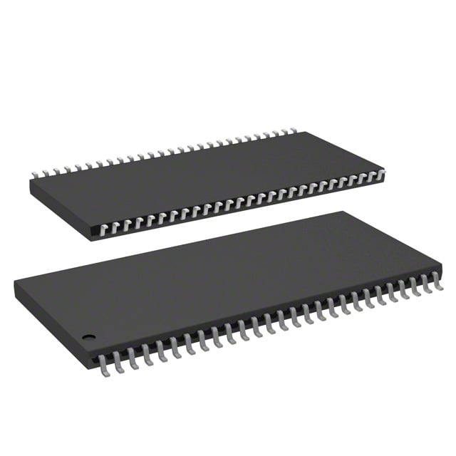
IS42S16400F-6TL-TR
| Part Description |
IC DRAM 64MBIT PAR 54TSOP II |
|---|---|
| Quantity | 194 Available (as of June 15, 2026) |

| Product Category | Memory |
|---|---|
| Manufacturer | Integrated Silicon Solution Inc |
| Manufacturing Status | Obsolete |
| Manufacturer Standard Lead Time | Contact Us |
| Datasheet |
Specifications & Environmental
| Device Package | 54-TSOP II | Memory Format | DRAM | Technology | SDRAM | ||
|---|---|---|---|---|---|---|---|
| Memory Size | 64 Mbit | Access Time | 5.4 ns | Grade | Commercial | ||
| Clock Frequency | 166 MHz | Voltage | 3V ~ 3.6V | Memory Type | Volatile | ||
| Operating Temperature | 0°C ~ 70°C (TA) | Write Cycle Time Word Page | N/A | Packaging | 54-TSOP (0.400", 10.16mm Width) | ||
| Mounting Method | Volatile | Memory Interface | Parallel | Memory Organization | 4M x 16 | ||
| Moisture Sensitivity Level | 3 (168 Hours) | RoHS Compliance | ROHS3 Compliant | REACH Compliance | REACH Unaffected | ||
| Qualification | N/A | ECCN | EAR99 | HTS Code | 8542.32.0002 |
Overview of IS42S16400F-6TL-TR – 64Mbit SDRAM, 54‑pin TSOP II
The IS42S16400F-6TL-TR is a 64 Mbit synchronous DRAM organized as 1,048,576 × 16 × 4 banks. It implements a pipelined, fully synchronous architecture to support high-speed parallel memory access with programmable burst and latency options.
Designed for commercial-temperature systems, this device targets designs that require a compact 54‑pin TSOP II footprint, single 3.3 V power supply operation, and clocked SDRAM performance up to 166 MHz.
Key Features
- Memory Organization — 64 Mbit arranged as 4M × 16 (1M × 16 × 4 banks) to support multi-bank operation and improved throughput.
- Synchronous SDRAM Core — Fully synchronous operation with all signals referenced to the rising edge of the clock; pipelined architecture for high-speed data transfer.
- Clock and Timing — Rated for a 166 MHz clock frequency (–6 speed grade) with access times down to 5.4 ns (CAS latency = 3) and programmable CAS latency options (2 or 3 clocks).
- Burst and Sequencing — Programmable burst lengths (1, 2, 4, 8, full page) and selectable burst sequence (sequential/interleave) with burst read/write and burst read/single write capability.
- Refresh and Power — Auto and self-refresh modes with 4096 refresh cycles per 64 ms (commercial/independent/A1 grade) or 4096 per 16 ms for A2 grade; single 3.3 V supply (3.0 V–3.6 V).
- Interface — LVTTL-compatible interface for standard parallel SDRAM signaling.
- Package and Temperature — 54‑pin TSOP II package (0.400", 10.16 mm width) specified for commercial operating temperature range 0°C to +70°C (TA).
- Bank Architecture — Internal bank structure to hide row access/precharge and enable random column access every clock cycle for flexible data handling.
Typical Applications
- Parallel SDRAM system memory — Used where 64 Mbit of synchronous DRAM in a 54‑pin TSOP II footprint is required for high-speed parallel access.
- Data buffering — Suitable for designs that need burst read/write buffering with programmable burst lengths and sequences.
- Embedded commercial electronics — Fits commercial-temperature embedded designs requiring a single 3.3 V SDRAM solution.
Unique Advantages
- High-speed, clocked operation: 166 MHz rated clock frequency (–6 grade) and 5.4 ns access time (CAS = 3) enable fast synchronous data transfers.
- Flexible performance tuning: Programmable CAS latency (2 or 3), burst lengths, and burst sequencing let designers optimize latency and throughput for target workloads.
- Efficient bank management: Four internal banks and internal row access/precharge hiding improve effective throughput for random and burst accesses.
- Standard 3.3 V supply: Operates from 3.0 V to 3.6 V for straightforward integration into existing 3.3 V systems.
- Compact TSOP II footprint: 54‑pin TSOP II (0.400", 10.16 mm width) offers a space-efficient package for board-level implementations.
- Refresh control options: Supports auto-refresh and self-refresh modes with defined refresh cycle counts, simplifying system-level power and data-retention management.
Why Choose IC DRAM 64MBIT PAR 54TSOP II?
The IS42S16400F-6TL-TR positions itself as a practical, compact SDRAM device for commercial embedded systems that require 64 Mbit of synchronous, banked memory in a 54‑pin TSOP II package. Its programmable latency, burst control, and internal bank architecture provide designers with the control needed to balance latency and throughput for varied memory workloads.
This device is suited to designs that need a standard 3.3 V parallel SDRAM solution with commercial temperature rating and predictable timing characteristics. Its combination of clocked operation, refresh modes, and compact package supports scalable integration into space-constrained PCBs and existing 3.3 V memory subsystems.
If you need pricing, availability, or a formal quote for IS42S16400F-6TL-TR, submit a parts inquiry or request a quote from your preferred supplier to receive ordering and lead-time information.