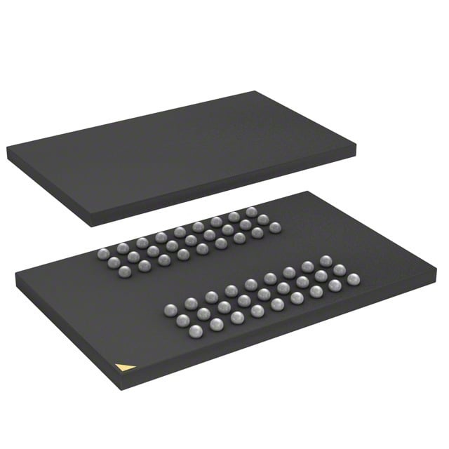
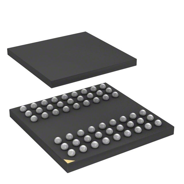
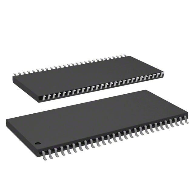
IS42S16800D-75ETLI
| Part Description |
IC DRAM 128MBIT PAR 54TSOP II |
|---|---|
| Quantity | 1,272 Available (as of June 14, 2026) |
| Product Category | Memory |
|---|---|
| Manufacturer | Integrated Silicon Solution Inc |
| Manufacturing Status | Obsolete |
| Manufacturer Standard Lead Time | Contact Us |
| Datasheet |
Specifications & Environmental
| Device Package | 54-TSOP II | Memory Format | DRAM | Technology | SDRAM | ||
|---|---|---|---|---|---|---|---|
| Memory Size | 128 Mbit | Access Time | 6.5 ns | Grade | Industrial | ||
| Clock Frequency | 133 MHz | Voltage | 3V ~ 3.6V | Memory Type | Volatile | ||
| Operating Temperature | -40°C ~ 85°C (TA) | Write Cycle Time Word Page | N/A | Packaging | 54-TSOP (0.400", 10.16mm Width) | ||
| Mounting Method | Volatile | Memory Interface | Parallel | Memory Organization | 8M x 16 | ||
| Moisture Sensitivity Level | 3 (168 Hours) | RoHS Compliance | ROHS3 Compliant | REACH Compliance | REACH Unaffected | ||
| Qualification | N/A | ECCN | EAR99 | HTS Code | 8542.32.0002 |
Overview of IS42S16800D-75ETLI – IC DRAM 128MBIT PAR 54TSOP II
The IS42S16800D-75ETLI is a 128‑Mbit synchronous DRAM (SDRAM) organized as 8M × 16 with a parallel LVTTL interface. It implements a quad‑bank, fully synchronous architecture optimized for high‑speed, burst‑oriented memory access.
Designed for systems requiring deterministic, clock‑referenced DRAM behavior, this device targets applications that benefit from programmable CAS latency, burst transfer modes and industrial temperature operation while running from a 3.0–3.6 V supply.
Key Features
- Memory Core 128 Mbit SDRAM organized as 8M × 16 (quad‑bank) providing 134,217,728 bits of storage.
- Synchronous SDRAM Architecture Fully synchronous operation with all signals referenced to the rising edge of CLK for predictable timing.
- Performance Clock frequency support including a 133 MHz variant for the -75E part; access time down to 6.5 ns (from clock) and programmable CAS latency (2, 3 clocks).
- Burst and Addressing Programmable burst length (1, 2, 4, 8, full page) and burst sequence (sequential/interleave); random column address capability every clock cycle.
- Refresh and Power Modes Auto Refresh (CBR), self refresh with programmable periods and 4096 refresh cycles every 64 ms to maintain data integrity.
- Interface and Signaling LVTTL‑compatible inputs/outputs and parallel memory interface for straightforward integration with synchronous controllers.
- Power Supply Operates from a 3.0 V to 3.6 V supply range.
- Package and Temperature 54‑pin TSOP II (0.400", 10.16 mm width) package with industrial temperature availability: –40 °C to 85 °C (TA).
Typical Applications
- Industrial Systems — Use in equipment requiring extended temperature operation and synchronous burst memory for deterministic data handling.
- Embedded Controllers — Local high‑speed SDRAM for embedded platforms that need programmable latency and burst transfer modes.
- Networking and Communications Modules — Buffering and temporary storage in clocked systems that leverage SDRAM burst capabilities and bank interleaving.
Unique Advantages
- Flexible Performance Options: Programmable CAS latency and multiple clock frequency variants enable tuning for latency or throughput per system requirements.
- Burst Transfer Efficiency: Programmable burst lengths and interleave/sequential modes allow efficient sustained data transfers and automatic column address generation.
- Robust Refresh Management: Auto and self‑refresh modes with defined refresh cycles (4096/64 ms) simplify power management while preserving data integrity.
- Industrial Temperature Range: Specified –40 °C to 85 °C operation supports deployment in temperature‑challenging environments.
- Compact Surface Package: 54‑pin TSOP II footprint delivers synchronous DRAM density in a small package suitable for space‑constrained board designs.
Why Choose IS42S16800D-75ETLI?
The IS42S16800D-75ETLI combines a synchronous, quad‑bank SDRAM architecture with programmable timing and burst features to deliver deterministic, high‑speed memory behavior in systems operating from a 3.0–3.6 V supply. Its 8M × 16 organization, 128 Mbit density and 54‑pin TSOP II package make it well suited for embedded and industrial designs that require predictable, burst‑oriented memory performance across a wide temperature range.
This device is appropriate for engineers and procurement teams seeking a verified synchronous DRAM building block with explicit refresh, latency and burst controls that map directly to system timing and power requirements.
Request a quote or submit an inquiry to receive pricing and availability information for the IS42S16800D-75ETLI.