IS42S16800D-7B
| Part Description |
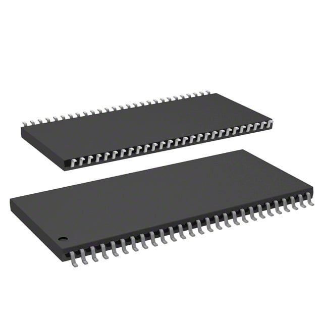
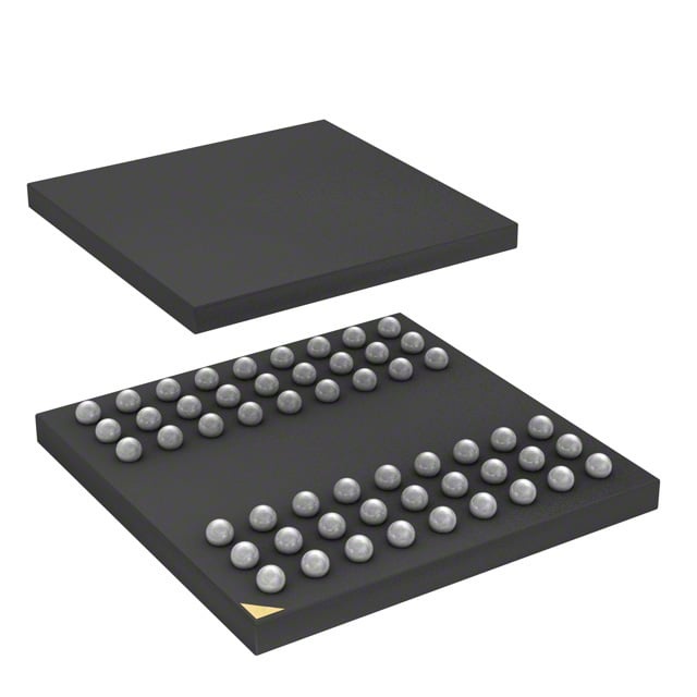
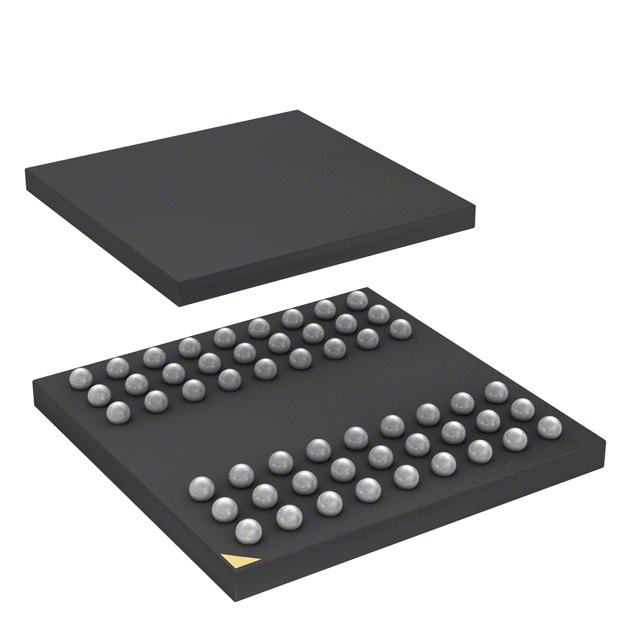
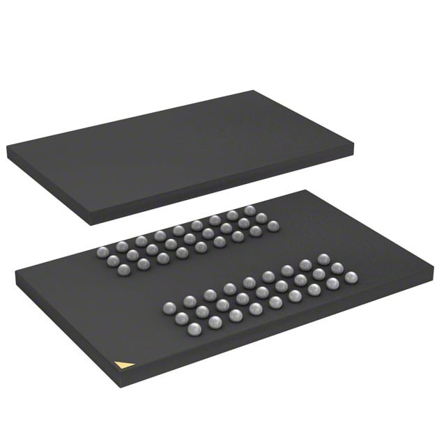
IC DRAM 128MBIT PAR 54MINIBGA |
|---|---|
| Quantity | 1,378 Available (as of June 15, 2026) |
| Product Category | Memory |
|---|---|
| Manufacturer | Integrated Silicon Solution Inc |
| Manufacturing Status | Obsolete |
| Manufacturer Standard Lead Time | Contact Us |
| Datasheet |
Specifications & Environmental
| Device Package | 54-MiniBGA (8x13) | Memory Format | DRAM | Technology | SDRAM | ||
|---|---|---|---|---|---|---|---|
| Memory Size | 128 Mbit | Access Time | 5.4 ns | Grade | Commercial | ||
| Clock Frequency | 143 MHz | Voltage | 3V ~ 3.6V | Memory Type | Volatile | ||
| Operating Temperature | 0°C ~ 70°C (TA) | Write Cycle Time Word Page | N/A | Packaging | 54-VFBGA | ||
| Mounting Method | Volatile | Memory Interface | Parallel | Memory Organization | 8M x 16 | ||
| Moisture Sensitivity Level | 3 (168 Hours) | RoHS Compliance | ROHS Compliant | REACH Compliance | REACH Unaffected | ||
| Qualification | N/A | ECCN | EAR99 | HTS Code | 8542.32.0002 |
Overview of IS42S16800D-7B – IC DRAM 128MBIT PAR 54MINIBGA
The IS42S16800D-7B is a 128 Mbit synchronous DRAM (SDRAM) organized as 8M × 16 with a parallel memory interface. It implements a quad-bank, fully synchronous pipeline architecture with LVTTL I/O and supports burst-oriented read/write operations and programmable timing modes.
Designed for 3.0–3.6 V systems (VDD/VDDQ 3.3 V nominal) and supplied in a 54-ball MiniBGA package, this device targets high-speed memory subsystems that require predictable burst performance, bank interleaving and standard SDRAM control features.
Key Features
- Core & architecture Quad-bank SDRAM with internal bank architecture to hide row access/precharge and enable interleaved bank operation for continuous burst transfers.
- Memory organization 128 Mbit capacity organized as 8M × 16 (2M × 16 × 4 banks), providing a standard parallel DRAM footprint for system memory expansion.
- Performance & timing Clock frequency up to 143 MHz for the -7 speed grade with access time from clock of 5.4 ns (CAS Latency = 3). Programmable CAS latency of 2 or 3 clocks.
- Burst & sequencing Programmable burst length (1, 2, 4, 8, full page) and selectable burst sequence (sequential or interleave) for flexible data transfer patterns.
- Refresh & power modes Supports Auto Refresh (CBR) and Self Refresh with programmable refresh periods; 4096 refresh cycles every 64 ms. Includes a low-power power-down mode.
- Interface & signaling LVTTL-compatible inputs/outputs and a parallel SDRAM interface for integration with standard 3.3 V memory controllers.
- Supply & package Operates from a 3.0–3.6 V supply (VDD/VDDQ nominal 3.3 V) and is offered in a 54-ball MiniBGA (8 × 13) package for compact board-level integration.
- Temperature range Specified operating temperature of 0°C to 70°C (TA); datasheet also notes industrial temperature availability.
Typical Applications
- High-speed memory subsystems Use as a synchronous DRAM device where burst transfers and bank interleaving are required for continuous data throughput.
- Embedded systems Integrate the 128 Mbit SDRAM into embedded designs that require a parallel 3.3 V SDRAM with programmable burst and CAS timings.
- Standard 3.3 V memory designs Suitable for systems designed around 3.3 V VDD/VDDQ with LVTTL signaling and compact MiniBGA packaging constraints.
Unique Advantages
- Predictable burst performance: Programmable burst lengths and sequences combined with CAS latency options deliver deterministic burst behavior for timing-sensitive designs.
- Bank interleaving for throughput: Quad-bank architecture and internal bank handling hide precharge delays and support seamless back-to-back accesses.
- Flexible refresh and low-power modes: Auto Refresh and Self Refresh with programmable periods plus power-down capability help manage system power and data integrity.
- Standard 3.3 V signaling: VDD/VDDQ nominal 3.3 V and LVTTL-compatible I/O simplify interfacing with existing 3.3 V memory controllers.
- Compact board-level package: 54-ball MiniBGA (8 × 13) enables space-efficient placement in designs with limited PCB area.
Why Choose IS42S16800D-7B?
The IS42S16800D-7B provides a factual combination of 128 Mbit SDRAM capacity, quad-bank architecture and programmable timing that suits designs requiring synchronous burst memory with predictable timing and refresh control. Its support for CAS latency options, multiple burst modes and LVTTL signaling makes it appropriate for systems built around a 3.3 V SDRAM interface.
This device is well suited to engineers and procurement teams specifying compact, parallel SDRAM in a 54-ball MiniBGA package who need documented performance parameters (143 MHz clock grade, 5.4 ns access from clock at CL=3) and standard SDRAM control features such as auto/self refresh and burst sequencing.
Request a quote or submit an inquiry to obtain pricing, availability and lead-time information for the IS42S16800D-7B.