IS42S16800E-6BL
| Part Description |
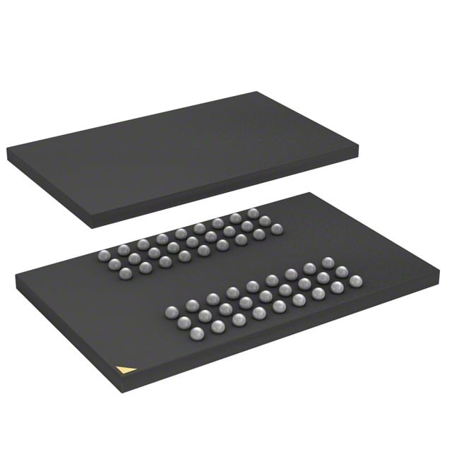
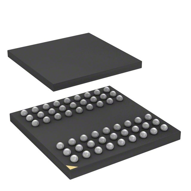
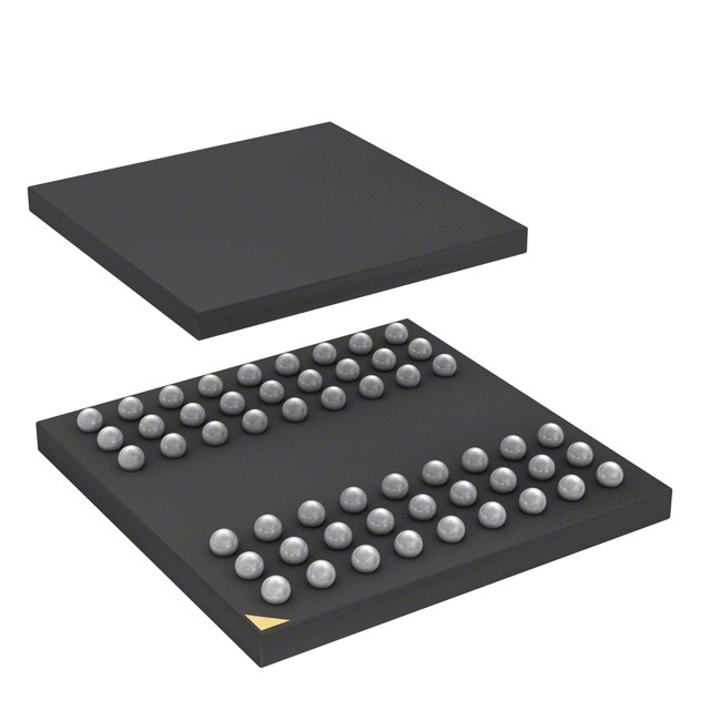
IC DRAM 128MBIT PAR 54TFBGA |
|---|---|
| Quantity | 440 Available (as of June 15, 2026) |

| Product Category | DRAM Memory |
|---|---|
| Manufacturer | Integrated Silicon Solution Inc |
| Manufacturing Status | Obsolete |
| Manufacturer Standard Lead Time | Contact Us |
| Datasheet |
Specifications & Environmental
| Device Package | 54-TFBGA (8x8) | Memory Format | DRAM | Technology | SDRAM | ||
|---|---|---|---|---|---|---|---|
| Memory Size | 128 Mbit | Access Time | 5.4 ns | Grade | Commercial | ||
| Clock Frequency | 166 MHz | Voltage | 3V ~ 3.6V | Memory Type | Volatile | ||
| Operating Temperature | 0°C ~ 70°C (TA) | Write Cycle Time Word Page | N/A | Packaging | 54-TFBGA | ||
| Mounting Method | Volatile | Memory Interface | Parallel | Memory Organization | 8M x 16 | ||
| Moisture Sensitivity Level | 3 (168 Hours) | RoHS Compliance | ROHS Compliant | REACH Compliance | REACH Unaffected | ||
| Qualification | N/A | ECCN | EAR99 | HTS Code | 8542.32.0002 |
Overview of IS42S16800E-6BL – IC DRAM 128MBIT PAR 54TFBGA
The IS42S16800E-6BL is a 128 Mbit synchronous DRAM (SDRAM) from Integrated Silicon Solution, Inc., organized internally as quad-bank memory and provided in a 54-ball TF‑BGA package. It delivers fully synchronous, parallel memory operation with LVTTL signaling and programmable burst modes for controlled data transfer behavior.
This device is intended for system designs that require 128 Mbit of volatile synchronous DRAM with a 166 MHz clock option, supporting short access times and features for refresh and low-power modes.
Key Features
- Memory Architecture 128 Mbit SDRAM organized as 8M × 16 (2M × 16 × 4 banks internally), implemented as a quad‑bank DRAM for pipelined access and bank interleaving.
- Performance Supports a 166 MHz clock option with a typical access time of 5.4 ns (CAS latency = 3) for fast read/write responsiveness.
- Programmable Burst and CAS Programmable burst lengths (1, 2, 4, 8, full page) and burst sequences (sequential/interleave), plus selectable CAS latency of 2 or 3 clocks.
- Refresh and Power Modes Auto Refresh and Self Refresh supported with 4096 refresh cycles every 64 ms; includes power-saving power-down capability.
- Interface and Signaling Fully synchronous operation with all signals referenced to the rising clock edge and LVTTL input/output signaling for parallel memory buses.
- Supply and Operating Range Operates from 3.0 V to 3.6 V supply and specified for an ambient operating temperature range of 0°C to 70°C (TA).
- Package Supplied in a 54‑TFBGA (8 × 8) package suitable for compact board designs.
Typical Applications
- High‑speed temporary storage Provides synchronous volatile storage for systems requiring rapid, clock‑aligned read/write operations.
- Memory buffering Used as a parallel SDRAM buffer to support burst transfer patterns and low-latency access in memory subsystems.
- Synchronous bus designs Integrates into designs that rely on LVTTL‑referenced, clocked memory interfaces and programmable burst behavior.
Unique Advantages
- Deterministic low-latency access 5.4 ns access time at CAS latency = 3 (166 MHz option) enables predictable timing for clocked memory systems.
- Flexible burst control Programmable burst lengths and sequences allow tuning of transfer patterns to match system throughput requirements.
- Quad‑bank pipelining Internal bank architecture hides row access/precharge and improves effective throughput for interleaved access.
- On‑chip refresh management Auto Refresh and Self Refresh support with 4096 cycles per 64 ms simplifies system refresh handling and power management.
- Compact TF‑BGA footprint 54‑ball TF‑BGA (8 × 8) package reduces board area for applications with constrained PCB space.
- Voltage compatibility 3.0 V to 3.6 V supply range aligns with standard 3.3 V memory system voltages for straightforward integration.
Why Choose IC DRAM 128MBIT PAR 54TFBGA?
The IS42S16800E-6BL positions itself as a compact, fully synchronous 128 Mbit DRAM solution offering programmable burst modes, selectable CAS latency, and on‑chip refresh features. Its quad‑bank architecture and 166 MHz option provide the timing characteristics needed for clocked parallel memory designs that require predictable access behavior.
This device is suited to designers seeking a defined specification for 128 Mbit volatile memory in a 54‑TFBGA package with LVTTL signaling and a 0°C to 70°C operating range. The combination of burst programmability, refresh management, and a standard 3.3 V class supply supports integration into systems that demand synchronous parallel DRAM functionality.
Request a quote or submit an inquiry for IS42S16800E-6BL to obtain pricing and availability details for your project needs.