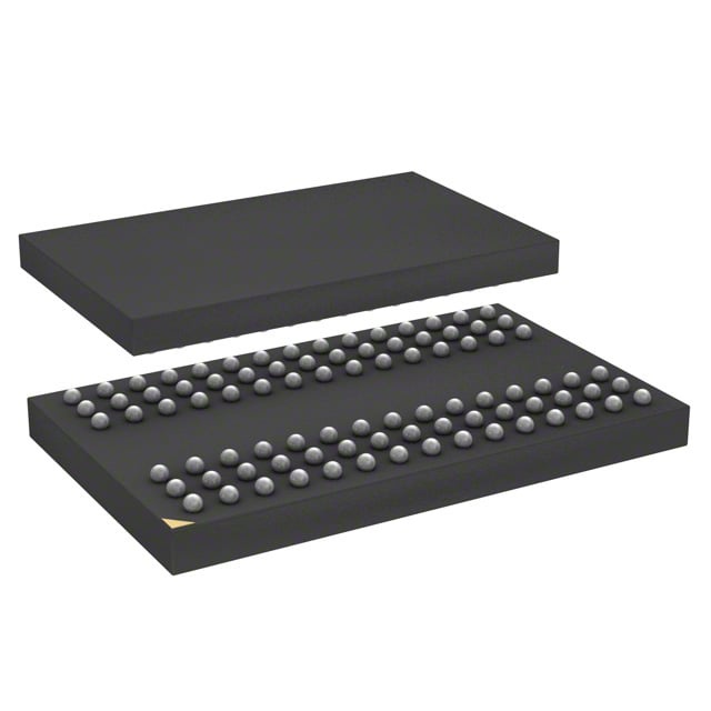
IS42S32200C1-7BI
| Part Description |
IC DRAM 64MBIT PAR 90BGA |
|---|---|
| Quantity | 81 Available (as of June 15, 2026) |

| Product Category | Memory |
|---|---|
| Manufacturer | Integrated Silicon Solution Inc |
| Manufacturing Status | Obsolete |
| Manufacturer Standard Lead Time | Contact Us |
| Datasheet |
Specifications & Environmental
| Device Package | 90-BGA (13x8) | Memory Format | DRAM | Technology | SDRAM | ||
|---|---|---|---|---|---|---|---|
| Memory Size | 64 Mbit | Access Time | 5.5 ns | Grade | Industrial | ||
| Clock Frequency | 143 MHz | Voltage | 3.15V ~ 3.45V | Memory Type | Volatile | ||
| Operating Temperature | -40°C ~ 85°C (TA) | Write Cycle Time Word Page | N/A | Packaging | 90-LFBGA | ||
| Mounting Method | Volatile | Memory Interface | Parallel | Memory Organization | 2M x 32 | ||
| Moisture Sensitivity Level | 3 (168 Hours) | RoHS Compliance | ROHS Compliant | REACH Compliance | REACH Unaffected | ||
| Qualification | N/A | ECCN | EAR99 | HTS Code | 8542.32.0002 |
Overview of IS42S32200C1-7BI – IC DRAM 64MBIT PAR 90BGA
The IS42S32200C1-7BI is a 64‑Mbit synchronous DRAM (SDRAM) organized as 512K × 32 × 4 banks, designed for high‑speed parallel memory applications. It implements a fully synchronous interface with internal bank architecture and LVTTL-compatible signaling for use in 3.3 V memory systems.
This device targets systems requiring buffered, burst-oriented data transfers and precise timing control — including applications that benefit from programmable burst lengths, programmable CAS latency, and industrial temperature operation.
Key Features
- Memory Architecture 64 Mbit SDRAM organized as 512K × 32 × 4 banks (2M × 32 organization), supporting internal bank interleaving to hide row precharge.
- Synchronous Performance Fully synchronous design with clocked inputs and outputs; specified for a primary clock option of 143 MHz (part -7) with access time as low as 5.5 ns (CAS latency = 3).
- Programmable Burst and Latency Programmable burst lengths (1, 2, 4, 8, full page), selectable burst sequence (sequential/interleave), and programmable CAS latency options (2 or 3 clocks).
- Refresh and Power Modes Supports AUTO REFRESH, SELF REFRESH and power‑down modes; specification includes 4096 refresh cycles every 64 ms for data integrity.
- Interface and Voltage Parallel memory interface with LVTTL-compatible signals and single supply operation across 3.15 V to 3.45 V (nominal 3.3 V).
- Package and Mounting 90‑ball LFBGA package (90-BGA, 13 × 8 ball array) for compact board mounting.
- Operating Temperature Industrial temperature grade: −40 °C to +85 °C (TA).
Typical Applications
- Embedded system memory High‑speed parallel SDRAM for system memory or local buffering in embedded controllers and single‑board computers.
- Industrial equipment Use in industrial controls and instrumentation that require extended temperature operation (−40 °C to +85 °C).
- Data buffering and burst transfers Applications needing burst read/write capability and programmable latency for predictable, high‑throughput transfers.
Unique Advantages
- Synchronous, predictable timing: Clocked operation and programmable CAS latency enable deterministic read/write timing for system designers.
- Flexible burst control: Multiple burst lengths and sequence modes let designers optimize throughput for sequential or interleaved accesses.
- Quad‑bank architecture: Four internal banks allow precharge hiding and improved random access performance without external arbitration changes.
- Robust refresh management: Built‑in AUTO and SELF REFRESH modes with defined refresh cycles (4096/64 ms) simplify memory maintenance and power management.
- Industrial temperature rating: Specified operation from −40 °C to +85 °C supports deployment in thermally demanding environments.
- Compact BGA footprint: 90‑ball LFBGA package reduces PCB area while providing a standard ball array for automated assembly.
Why Choose IC DRAM 64MBIT PAR 90BGA?
The IS42S32200C1-7BI provides a straightforward, fully synchronous 64‑Mbit SDRAM solution for designs that require parallel data throughput, programmable burst behavior, and industrial temperature operation. Its single 3.3 V supply, LVTTL interface, and quad‑bank organization make it suitable for embedded systems and equipment needing reliable, burst‑oriented memory.
Engineers specifying this device benefit from clear timing parameters (including CAS latency options and access times), integrated refresh handling, and a compact 90‑ball LFBGA package — all documented in the device specification from the manufacturer, Integrated Silicon Solution, Inc.
Request a quote or submit an inquiry for IS42S32200C1-7BI to obtain pricing and availability information.