IS42S32200C1-7BL-TR
| Part Description |
IC DRAM 64MBIT PAR 90BGA |
|---|---|
| Quantity | 583 Available (as of June 15, 2026) |
| Product Category | Memory |
|---|---|
| Manufacturer | Integrated Silicon Solution Inc |
| Manufacturing Status | Obsolete |
| Manufacturer Standard Lead Time | Contact Us |
| Datasheet |
Specifications & Environmental
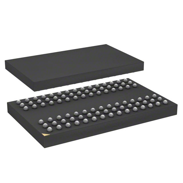
| Device Package | 90-BGA (13x8) | Memory Format | DRAM | Technology | SDRAM | ||
|---|---|---|---|---|---|---|---|
| Memory Size | 64 Mbit | Access Time | 5.5 ns | Grade | Commercial | ||
| Clock Frequency | 143 MHz | Voltage | 3.15V ~ 3.45V | Memory Type | Volatile | ||
| Operating Temperature | 0°C ~ 70°C (TA) | Write Cycle Time Word Page | N/A | Packaging | 90-LFBGA | ||
| Mounting Method | Volatile | Memory Interface | Parallel | Memory Organization | 2M x 32 | ||
| Moisture Sensitivity Level | 3 (168 Hours) | RoHS Compliance | ROHS3 Compliant | REACH Compliance | REACH Unaffected | ||
| Qualification | N/A | ECCN | EAR99 | HTS Code | 8542.32.0002 |
Overview of IS42S32200C1-7BL-TR – 64 Mbit SDRAM, 90‑Ball BGA, 143 MHz
The IS42S32200C1-7BL-TR is a 64‑Mbit synchronous DRAM (SDRAM) device from Integrated Silicon Solution Inc (ISSI), organized internally as 524,288 × 32 bits across four banks (2M × 32). It is a fully synchronous DRAM designed for 3.3 V memory systems with LVTTL signaling and a pipeline architecture to support high‑speed burst transfers.
This package variant is supplied in a 90‑ball BGA (13 × 8) and is specified for operation at up to 143 MHz with an access time of 5.5 ns, making it suitable for designs requiring synchronous, burst‑oriented memory with programmable timing and refresh control.
Key Features
- Core/Architecture Quad‑bank SDRAM architecture with internal bank interleaving to hide row access and precharge times for efficient burst access.
- Memory Organization & Capacity 64 Mbit total capacity organized as 524,288 × 32 bits (2M × 32) across four banks.
- Performance & Timing Rated for 143 MHz operation (this part variant) with an access time of 5.5 ns and programmable CAS latency options (2 or 3 clocks) as documented in the device datasheet.
- Burst & Sequencing Programmable burst lengths (1, 2, 4, 8, full page) and selectable sequential or interleave burst sequences for flexible data transfer patterns.
- Refresh & Power Modes Supports self‑refresh, AUTO REFRESH mode, and power‑down modes; specified for 4096 refresh cycles every 64 ms.
- Interface & Signaling Fully synchronous interface with all signals referenced to the rising clock edge and LVTTL‑compatible I/O.
- Supply Voltage Single 3.3 V supply range specified as 3.15 V to 3.45 V.
- Package & Temperature 90‑ball LFBGA (13 × 8) package. Operating ambient temperature specified as 0 °C to 70 °C (TA). The device family is also noted in the datasheet as available in industrial temperature grade and lead‑free options.
Typical Applications
- 3.3 V Memory Subsystems Drop‑in synchronous DRAM for 3.3 V memory system designs that require burst read/write capability and LVTTL signaling.
- High‑speed Data Buffering Use where pipeline architecture and programmable burst lengths are needed to sustain high‑rate, sequential data transfers.
- Systems Requiring Self‑Refresh Designs that benefit from self‑refresh and AUTO REFRESH modes to maintain data retention while minimizing active power.
Unique Advantages
- Flexible Burst Control: Programmable burst lengths and selectable burst sequencing allow tuning of transfers to match system access patterns.
- Synchronous Pipeline Architecture: All signals registered to the rising clock edge support predictable timing and straightforward integration into synchronous memory buses.
- Bank Interleaving: Quad‑bank organization enables precharging of one bank while accessing another to improve effective throughput during random access patterns.
- Multiple Timing Options: Programmable CAS latency (2 or 3) and available speed grades (including the 143 MHz grade for this part) provide options for balancing latency and clock speed.
- Compact BGA Package: 90‑ball LFBGA (13 × 8) package provides a compact form factor for space‑constrained board designs.
Why Choose IS42S32200C1-7BL-TR?
The IS42S32200C1-7BL-TR delivers a synchronous, burst‑oriented 64‑Mbit SDRAM solution with quad‑bank architecture, programmable timing, and self‑refresh capabilities suitable for 3.3 V memory systems. Its 90‑ball BGA packaging and documented timing grades make it a practical choice for designers seeking a compact, high‑performance SDRAM building block.
This device is appropriate for projects that require predictable synchronous timing, flexible burst behavior, and power management features such as self‑refresh. The combination of programmable CAS latency, bank interleaving, and supported refresh modes supports both throughput and low‑power design considerations as documented in the product datasheet.
Request a quote or submit a product inquiry for IS42S32200C1-7BL-TR to receive pricing and availability details for your design and procurement needs.