IS42S32200C1-7B
| Part Description |
IC DRAM 64MBIT PAR 90BGA |
|---|---|
| Quantity | 556 Available (as of June 14, 2026) |

| Product Category | Memory |
|---|---|
| Manufacturer | Integrated Silicon Solution Inc |
| Manufacturing Status | Obsolete |
| Manufacturer Standard Lead Time | Contact Us |
| Datasheet |
Specifications & Environmental
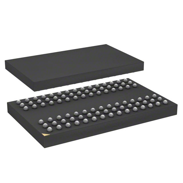
| Device Package | 90-BGA (13x8) | Memory Format | DRAM | Technology | SDRAM | ||
|---|---|---|---|---|---|---|---|
| Memory Size | 64 Mbit | Access Time | 5.5 ns | Grade | Commercial | ||
| Clock Frequency | 143 MHz | Voltage | 3.15V ~ 3.45V | Memory Type | Volatile | ||
| Operating Temperature | 0°C ~ 70°C (TA) | Write Cycle Time Word Page | N/A | Packaging | 90-LFBGA | ||
| Mounting Method | Volatile | Memory Interface | Parallel | Memory Organization | 2M x 32 | ||
| Moisture Sensitivity Level | 3 (168 Hours) | RoHS Compliance | ROHS3 Compliant | REACH Compliance | REACH Unaffected | ||
| Qualification | N/A | ECCN | EAR99 | HTS Code | 8542.32.0002 |
Overview of IS42S32200C1-7B – IC DRAM 64MBIT PAR 90BGA
The IS42S32200C1-7B is a 64‑Mbit synchronous DRAM organized as 2M × 32 with internal four‑bank architecture for high‑throughput, pipelined memory access. It is a 3.3V LVTTL‑interface parallel SDRAM supplied in a 90‑ball LFBGA package and intended for systems requiring a compact 64‑Mbit volatile memory solution.
This device targets applications that need synchronous burst reads/writes, programmable burst lengths and sequences, and predictable timing at the specified 143 MHz speed grade (CAS‑3 timing). Its architecture supports bank interleaving and auto precharge to help hide row access and precharge latency.
Key Features
- Memory Organization 64‑Mbit capacity organized internally as 524,288 × 32 × 4 banks (each bank: 2,048 rows × 256 columns × 32 bits), enabling quad‑bank operation and interleaving.
- SDRAM / Synchronous Interface Fully synchronous SDRAM with all inputs and outputs referenced to the positive clock edge and LVTTL compatible signaling.
- Speed Grade and Timing 143 MHz clock frequency (‑7 speed grade) with CAS latency programmable to 2 or 3 cycles; specified access time of 5.5 ns for CAS‑3 operation.
- Burst and Sequencing Programmable burst length (1, 2, 4, 8, full page) and selectable burst sequence (sequential or interleave) for flexible data transfer patterns.
- Refresh and Power Modes Supports AUTO REFRESH and self‑refresh modes with 4,096 refresh cycles every 64 ms, plus power‑down capability.
- Power Supply Single 3.3 V supply with an operating voltage range of 3.15 V to 3.45 V.
- Package and Temperature Available in a 90‑ball LFBGA (13 × 8) package; specified operating ambient temperature 0 °C to 70 °C (TA).
- Burst Control and Termination Supports burst termination via burst stop and precharge commands and allows random column address changes every clock cycle during burst access.
- Manufacturing Options Datasheet notes availability in lead‑free packages and in other package/temperature grades (device options documented in the specification).
Typical Applications
- Embedded Memory Subsystems Use as a system DRAM for embedded controllers and processors requiring a 64‑Mbit synchronous parallel memory.
- High‑Speed Buffering Suitable for buffering and burst data transfer where predictable CAS‑3 timing at 143 MHz is required.
- Compact Board Designs The 90‑ball LFBGA package enables space‑constrained PCBs that need surface‑mount SDRAM in a small footprint.
Unique Advantages
- Quad‑Bank Architecture: Four internal banks allow bank interleaving to hide precharge time and improve sustained throughput in burst operations.
- Flexible Burst Control: Programmable burst length and sequence options simplify integration with a variety of bus controllers and access patterns.
- Predictable Timing: Defined CAS latency options (2 or 3) and specified access times (5.5 ns at CAS‑3) support deterministic performance tuning.
- Standard 3.3V Interface: Single 3.3 V supply and LVTTL signaling simplify power and I/O planning in 3.3V memory systems.
- Compact BGA Package: 90‑ball LFBGA (13×8) provides a low‑profile, board‑space efficient package for compact designs.
Why Choose IS42S32200C1-7B?
The IS42S32200C1-7B combines a synchronous LVTTL interface, quad‑bank SDRAM architecture, and programmable burst and CAS settings to deliver a compact 64‑Mbit DRAM solution with predictable timing and flexible access modes. Its 3.3 V operation, support for self‑refresh and auto refresh, and 90‑ball LFBGA packaging make it suitable for embedded systems and applications that require a small form‑factor parallel SDRAM with defined performance at the 143 MHz speed grade.
Choose this device when your design requires a straightforward, documented 64‑Mbit SDRAM option with programmable burst behavior, bank interleaving, and standard 3.3 V LVTTL interfacing for integration into existing memory subsystems.
Request a quote or contact sales to submit a product inquiry and receive pricing and availability information for the IS42S32200C1-7B.