IS42S32200C1-6TLI-TR
| Part Description |
IC DRAM 64MBIT PAR 86TSOP II |
|---|---|
| Quantity | 456 Available (as of June 18, 2026) |

| Product Category | DRAM Memory |
|---|---|
| Manufacturer | Integrated Silicon Solution Inc |
| Manufacturing Status | Obsolete |
| Manufacturer Standard Lead Time | Contact Us |
| Datasheet |
Specifications & Environmental
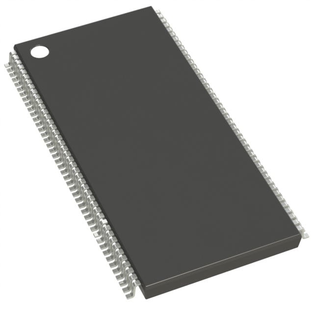
| Device Package | 86-TSOP II | Memory Format | DRAM | Technology | SDRAM | ||
|---|---|---|---|---|---|---|---|
| Memory Size | 64 Mbit | Access Time | 5.5 ns | Grade | Industrial | ||
| Clock Frequency | 166 MHz | Voltage | 3.15V ~ 3.45V | Memory Type | Volatile | ||
| Operating Temperature | -40°C ~ 85°C (TA) | Write Cycle Time Word Page | N/A | Packaging | 86-TFSOP (0.400", 10.16mm Width) | ||
| Mounting Method | Volatile | Memory Interface | Parallel | Memory Organization | 2M x 32 | ||
| Moisture Sensitivity Level | 3 (168 Hours) | RoHS Compliance | ROHS3 Compliant | REACH Compliance | REACH Unaffected | ||
| Qualification | N/A | ECCN | EAR99 | HTS Code | 8542.32.0002 |
Overview of IS42S32200C1-6TLI-TR – IC DRAM 64MBIT PAR 86TSOP II
The IS42S32200C1-6TLI-TR from Integrated Silicon Solution Inc. is a 64‑Mbit synchronous DRAM organized as 524,288 × 32 × 4 banks. It implements a fully synchronous, pipelined architecture with all signals referenced to the positive clock edge to support high‑speed parallel memory operations.
Designed for 3.3V memory systems, the device offers programmable burst lengths and CAS latency, LVTTL signaling, and industrial temperature operation (−40°C to 85°C), making it suitable for systems requiring deterministic burst transfers and robust thermal range.
Key Features
- Memory Architecture Organized as 524,288 × 32 × 4 banks (64‑Mbit) with internal banking to hide row access/precharge and enable interleaved accesses.
- Speed and Timing Clock frequency options of 183, 166 and 143 MHz. The -6 grade (IS42S32200C1-6) supports 166 MHz operation with typical access time of 5.5 ns (CAS latency = 3).
- Fully Synchronous Interface All inputs and outputs are registered on the rising edge of CLK; LVTTL compatible signaling for parallel memory interfaces.
- Burst and CAS Control Programmable burst lengths (1, 2, 4, 8, full page) and programmable burst sequence (sequential or interleave). CAS latency options: 2 or 3 clocks.
- Refresh and Power Management Supports AUTO REFRESH and self‑refresh modes with 4096 refresh cycles every 64 ms. Single 3.3V power supply; voltage supply range 3.15 V to 3.45 V.
- Package and Temperature Available in 86‑TSOP II (400‑mil, 10.16 mm width) and 90‑ball BGA options; specified operating range −40°C to 85°C. Lead‑free package options available.
Typical Applications
- 3.3V Memory Systems Acts as parallel DRAM memory in systems designed around a 3.3V supply and synchronous clocked memory interfaces.
- Industrial Equipment Operation from −40°C to 85°C and available industrial grade packaging suit industrial control and instrumentation environments.
- High‑Speed Burst Buffering Programmable burst lengths, CAS latency options and quad‑bank interleave enable deterministic burst read/write transfers and buffering in high‑throughput designs.
Unique Advantages
- Quad‑bank Architecture for Throughput: Internal four‑bank configuration enables bank interleaving to hide precharge time and sustain continuous burst accesses.
- Flexible Timing Control: Programmable CAS latency (2 or 3) and selectable burst lengths/sequences allow designers to tune performance to system timing requirements.
- Synchronous LVTTL Interface: Registered I/O on the rising clock edge with LVTTL signaling simplifies integration into synchronous parallel memory subsystems.
- Industrial Temperature Range: Specified −40°C to 85°C operation supports deployment in thermally demanding or outdoor environments.
- Standard 3.3V Supply Compatibility: Single 3.3V power supply with defined voltage window (3.15 V–3.45 V) for straightforward power system design.
Why Choose IS42S32200C1-6TLI-TR?
The IS42S32200C1-6TLI-TR delivers a compact 64‑Mbit SDRAM solution with programmable timing, burst control and quad‑bank architecture to support high‑speed, deterministic parallel memory designs. Its LVTTL synchronous interface and 3.3V compatibility make it a direct fit for systems that require predictable burst transfers and simple clocked integration.
With industrial temperature capability and available lead‑free packaging, this ISSI device is suited to applications where thermal range and package options matter. It is appropriate for engineers specifying reliable, configurable SDRAM for embedded and industrial memory subsystems.
Request a quote or submit an inquiry to obtain pricing, availability and lead‑time information for IS42S32200C1-6TLI-TR.