IS42S32200C1-6TL
| Part Description |
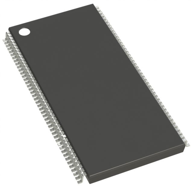
IC DRAM 64MBIT PAR 86TSOP II |
|---|---|
| Quantity | 734 Available (as of June 15, 2026) |

| Product Category | Memory |
|---|---|
| Manufacturer | Integrated Silicon Solution Inc |
| Manufacturing Status | Obsolete |
| Manufacturer Standard Lead Time | Contact Us |
| Datasheet |
Specifications & Environmental
| Device Package | 86-TSOP II | Memory Format | DRAM | Technology | SDRAM | ||
|---|---|---|---|---|---|---|---|
| Memory Size | 64 Mbit | Access Time | 5.5 ns | Grade | Commercial | ||
| Clock Frequency | 166 MHz | Voltage | 3.15V ~ 3.45V | Memory Type | Volatile | ||
| Operating Temperature | 0°C ~ 70°C (TA) | Write Cycle Time Word Page | N/A | Packaging | 86-TFSOP (0.400", 10.16mm Width) | ||
| Mounting Method | Volatile | Memory Interface | Parallel | Memory Organization | 2M x 32 | ||
| Moisture Sensitivity Level | 3 (168 Hours) | RoHS Compliance | ROHS3 Compliant | REACH Compliance | REACH Unaffected | ||
| Qualification | N/A | ECCN | EAR99 | HTS Code | 8542.32.0002 |
Overview of IS42S32200C1-6TL – IC DRAM 64MBIT PAR 86TSOP II
The IS42S32200C1-6TL is a 64-Mbit synchronous DRAM organized as 512K×32×4 (4 banks) that delivers high-speed, burst-oriented data transfers using a pipeline architecture. It is designed for 3.3V memory systems with an LVTTL interface and supports programmable burst lengths and sequences for flexible data access patterns.
This device is intended for use in systems that require synchronous, high-rate parallel memory access with internal bank interleaving and self-refresh capabilities to manage refresh cycles and power-saving modes.
Key Features
- Memory Architecture 64 Mbit SDRAM organized as 512K bits × 32 bits × 4 banks, enabling internal bank interleaving and improved random-access performance.
- Synchronous Pipeline Operation Fully synchronous design with all signals registered on the rising edge of CLK for predictable timing and pipelined data transfers.
- Clock and Timing Supported clock frequency grades include 183, 166, and 143 MHz. Programmable CAS latency options of 2 or 3 clocks and access times down to 5.5 ns (CAS latency = 3) are provided.
- Burst Control Programmable burst lengths (1, 2, 4, 8, full page) and burst sequence modes (sequential/interleave) with burst termination via burst stop or precharge command.
- Refresh and Power Modes Auto refresh and self-refresh modes with 4096 refresh cycles every 64 ms plus a power-down mode for reduced power during idle periods.
- Interface and Logic Levels LVTTL-compatible input/output signaling and a single 3.3V power supply (specified supply range 3.15 V to 3.45 V).
- Package and Temperature Available in a 86-pin TSOP II (400-mil, 10.16 mm width) package; device literature notes availability in industrial temperature grades. Specified commercial operating range is 0°C to 70°C (TA).
Typical Applications
- 3.3V memory subsystems Designed for systems operating with a 3.3V supply that require synchronous parallel DRAM for high-rate data transfers.
- High-speed burst data buffering Programmable burst lengths and pipeline architecture support burst-oriented read/write operations for burst buffering use cases.
- Systems requiring bank interleaving Quad-bank organization and internal precharge hiding enable reduced latency for random-access patterns across multiple banks.
Unique Advantages
- Quad-bank internal organization: Four internal banks allow precharge hiding and interleaving to improve effective throughput for staggered accesses.
- Flexible burst operation: Programmable burst length and sequence options let designers tailor transfers for sequential or interleaved data patterns.
- Multiple speed grades: Offered in 183/166/143 MHz clock grades with CAS latency options, enabling selection for specific timing requirements.
- Synchronous pipeline design: All signals referenced to the positive clock edge for consistent timing and predictable integration into synchronous memory systems.
- Standard 3.3V LVTTL interface: Simplifies interface design in 3.3V systems while supporting LVTTL signaling for compatibility with common logic families.
- Package options and temperature availability: Supplied in 86-pin TSOP II (400-mil) and noted as available in industrial temperature grades to match form-factor and thermal requirements.
Why Choose IS42S32200C1-6TL?
The IS42S32200C1-6TL provides a synchronous, pipelined 64-Mbit DRAM solution optimized for 3.3V memory systems that require programmable burst behavior, internal bank interleaving, and LVTTL I/O. Its multiple speed grades and CAS latency options let designers balance timing and throughput to meet system requirements.
This device is well suited for designs needing predictable, burst-oriented parallel memory with on-chip refresh management and package options for space-constrained board layouts. The documented timing parameters and supply range support engineering evaluation and integration into synchronous memory subsystems.
Request a quote or submit an inquiry to receive pricing and availability information for the IS42S32200C1-6TL.