IS42S32200C1-6T
| Part Description |
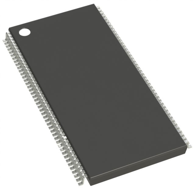
IC DRAM 64MBIT PAR 86TSOP II |
|---|---|
| Quantity | 613 Available (as of June 15, 2026) |

| Product Category | Memory |
|---|---|
| Manufacturer | Integrated Silicon Solution Inc |
| Manufacturing Status | Obsolete |
| Manufacturer Standard Lead Time | Contact Us |
| Datasheet |
Specifications & Environmental
| Device Package | 86-TSOP II | Memory Format | DRAM | Technology | SDRAM | ||
|---|---|---|---|---|---|---|---|
| Memory Size | 64 Mbit | Access Time | 5.5 ns | Grade | Commercial | ||
| Clock Frequency | 166 MHz | Voltage | 3.15V ~ 3.45V | Memory Type | Volatile | ||
| Operating Temperature | 0°C ~ 70°C (TA) | Write Cycle Time Word Page | N/A | Packaging | 86-TFSOP (0.400", 10.16mm Width) | ||
| Mounting Method | Volatile | Memory Interface | Parallel | Memory Organization | 2M x 32 | ||
| Moisture Sensitivity Level | 3 (168 Hours) | RoHS Compliance | ROHS3 Compliant | REACH Compliance | REACH Unaffected | ||
| Qualification | N/A | ECCN | EAR99 | HTS Code | 8542.32.0002 |
Overview of IS42S32200C1-6T – IC DRAM 64MBIT PAR 86TSOP II
The IS42S32200C1-6T is a 64‑Mbit synchronous DRAM (SDRAM) organized as 2M × 32 with four internal banks and a fully synchronous, pipelined architecture. It is designed for 3.3V memory systems and supports high-speed, burst-oriented data transfers with registered inputs and outputs referenced to the positive clock edge.
This device targets designs that require a parallel SDRAM with programmable burst lengths and sequences, selectable CAS latency, self-refresh and power-down modes, and compact 86‑TSOP II packaging for space‑constrained boards.
Key Features
- Memory 64 Mbit total capacity organized as 524,288 × 32 × 4 banks (2M × 32). Parallel DRAM format for synchronous, burst-oriented access.
- Performance Clock frequency options include 183, 166 and 143 MHz; programmable CAS latency of 2 or 3 clocks; access times down to 5.5 ns (CAS‑latency dependent).
- Burst and Sequencing Programmable burst lengths (1, 2, 4, 8, full page) and selectable burst sequence (sequential or interleave) for flexible data transfer patterns.
- Internal Banking & Precharge Four internal banks and internal bank management to hide row access/precharge; supports AUTO PRECHARGE and burst termination commands.
- Refresh & Power Self-refresh and power-down modes supported with 4096 refresh cycles every 64 ms to maintain data integrity.
- Interface LVTTL‑compatible inputs/outputs with fully synchronous operation referenced to the rising edge of CLK; random column address capability every clock cycle.
- Supply and Operating Range Single‑supply operation with VCC range 3.15 V to 3.45 V (3.3V system operation). Commercial operating temperature range: 0°C to 70°C; industrial temperature grade versions are available.
- Package Available in a 86‑pin TSOP II (400‑mil, 10.16 mm width) package for compact board-level integration; also offered in BGA variants per datasheet options.
Typical Applications
- Parallel SDRAM subsystems Used as system memory in designs that require 64‑Mbit synchronous DRAM with programmable burst transfer capabilities.
- High‑speed buffering Suited for buffer memory where burst reads/writes and random column access every clock cycle improve throughput.
- Memory expansion on 3.3V boards Integrates into 3.3V memory systems needing compact TSOP II packaging and standard LVTTL signaling.
Unique Advantages
- Flexible performance configurations: Multiple clock speed options (183/166/143 MHz) and selectable CAS latency (2 or 3) let designers balance speed and timing requirements.
- Burst and bank-level efficiency: Programmable burst lengths/sequences and four internal banks help maximize data throughput and hide precharge delays.
- Single 3.3V supply: Operates from a standard 3.15–3.45 V supply for easy integration into existing 3.3V memory subsystems.
- Power management features: Self‑refresh and power‑down modes reduce power during idle periods while maintaining data integrity with required refresh cycles.
- Compact package options: 86‑pin TSOP II (400‑mil) package enables high‑density board layouts where space is constrained.
Why Choose IC DRAM 64MBIT PAR 86TSOP II?
The IS42S32200C1‑6T delivers a verified 64‑Mbit SDRAM solution with synchronous, pipelined architecture and flexible timing options for designs that require burst‑oriented parallel memory. Its four‑bank organization, selectable CAS latency, and programmable burst behavior provide designers control over throughput and latency to match system requirements.
This device is suited for 3.3V memory systems that need a compact TSOP II package and advanced SDRAM features such as self‑refresh, power‑down, and internal bank precharge. Availability in commercial and industrial temperature grades and multiple package options supports a range of board‑level implementations and lifecycle requirements.
Request a quote or submit an inquiry to obtain product pricing, availability and lead‑time information for the IS42S32200C1‑6T.