IS42S32200C1-55T
| Part Description |
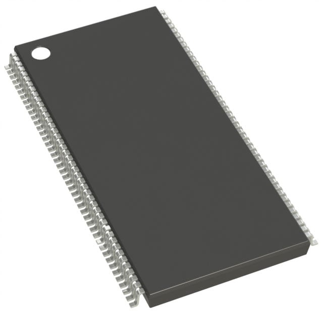
IC DRAM 64MBIT PAR 86TSOP II |
|---|---|
| Quantity | 1,066 Available (as of June 15, 2026) |

| Product Category | DRAM Memory |
|---|---|
| Manufacturer | Integrated Silicon Solution Inc |
| Manufacturing Status | Obsolete |
| Manufacturer Standard Lead Time | Contact Us |
| Datasheet |
Specifications & Environmental
| Device Package | 86-TSOP II | Memory Format | DRAM | Technology | SDRAM | ||
|---|---|---|---|---|---|---|---|
| Memory Size | 64 Mbit | Access Time | 5 ns | Grade | Commercial | ||
| Clock Frequency | 183 MHz | Voltage | 3.15V ~ 3.45V | Memory Type | Volatile | ||
| Operating Temperature | 0°C ~ 70°C (TA) | Write Cycle Time Word Page | N/A | Packaging | 86-TFSOP (0.400", 10.16mm Width) | ||
| Mounting Method | Volatile | Memory Interface | Parallel | Memory Organization | 2M x 32 | ||
| Moisture Sensitivity Level | 3 (168 Hours) | RoHS Compliance | ROHS Compliant | REACH Compliance | REACH Unaffected | ||
| Qualification | N/A | ECCN | EAR99 | HTS Code | 8542.32.0002 |
Overview of IS42S32200C1-55T – 64Mbit Synchronous DRAM (86‑TSOP II)
The IS42S32200C1-55T is a 64‑Mbit synchronous DRAM organized as 2M × 32 with four internal banks and a fully synchronous, clock‑referenced interface. It is designed for use in 3.3V memory systems requiring a parallel SDRAM with programmable burst and timing options.
This device targets systems that need deterministic, burst‑oriented memory access with features such as internal bank interleaving, self refresh, and programmable CAS latency to balance throughput and timing requirements.
Key Features
- Memory Capacity & Organization 64 Mbit total, internally configured as 524,288 × 32 × 4 banks (2,048 rows × 256 columns × 32 bits per bank).
- Synchronous Architecture Fully synchronous operation with all signals referenced to the rising edge of CLK for predictable timing.
- Performance Options Clock frequency options up to 183 MHz (other grades: 166, 143 MHz); programmable CAS latency (2 or 3 clocks) and access time down to 5 ns (CL=3).
- Burst & Sequencing Programmable burst lengths (1, 2, 4, 8, full page) and burst sequence modes (sequential or interleave); supports burst read/write and burst read/single write operations.
- Banking & Precharge Quad‑bank organization with internal bank interleaving to hide row access/precharge and AUTO PRECHARGE capability for self‑timed row precharge at burst end.
- Refresh & Power Modes Self refresh modes and 4,096 refresh cycles every 64 ms to maintain data integrity; power‑down mode supported.
- Interface & Signaling LVTTL compatible inputs/outputs and a parallel memory interface for synchronous system integration.
- Supply & Temperature Single 3.3V supply operation with recommended voltage range 3.15 V to 3.45 V; specified operating temperature 0°C to 70°C (TA). Datasheet notes an industrial temperature grade option is available.
- Package Available in a 86‑pin TSOP II (400‑mil, 10.16 mm width) package for standard board mounting and high‑density assembly.
Unique Advantages
- Deterministic synchronous timing: All signals are referenced to CLK, simplifying timing analysis and system integration for clocked designs.
- Flexible latency and burst control: Programmable CAS latency (2 or 3) and multiple burst lengths/sequences allow tuning for different throughput and latency tradeoffs.
- Improved effective throughput: Four internal banks with bank interleaving and AUTO PRECHARGE support reduce idle cycles from row precharge operations.
- Standard 3.3V single‑supply operation: Operates within a defined 3.15–3.45 V window for compatibility with common 3.3V memory systems.
- Robust refresh and low‑power modes: Self refresh and power‑down modes plus defined refresh scheduling (4,096 cycles/64 ms) help maintain data integrity while minimizing power.
- Industry‑standard package option: 86‑TSOP II footprint enables straightforward placement in compact board designs requiring a parallel SDRAM solution.
Why Choose IS42S32200C1-55T?
The IS42S32200C1-55T delivers a balanced set of synchronous DRAM features—quad‑bank architecture, programmable CAS latency and burst modes, and up to 183 MHz operation—packaged in an 86‑pin TSOP II. These characteristics make it suitable for systems that require predictable, burst‑oriented parallel memory with selectable timing behavior.
Its single 3.3V supply, LVTTL signaling, refresh management and available industrial temperature option provide designers with a practical, specification‑driven memory component that can be matched to a range of synchronous memory system requirements while relying on the detailed timing and operational parameters provided in the device datasheet.
Request a quote or submit an inquiry to obtain pricing, lead time, and availability information for the IS42S32200C1-55T. Provide your required order quantities and any specific temperature‑grade needs to receive a detailed response.