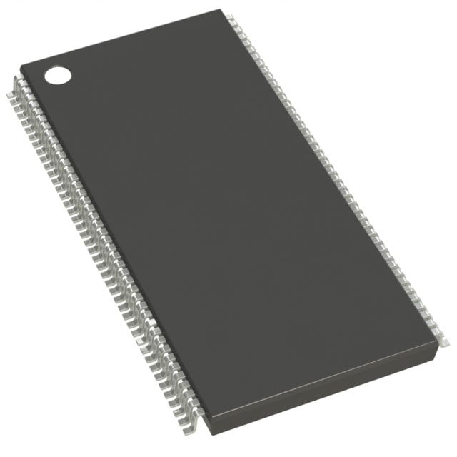
IS42S32200C1-7T-TR
| Part Description |
IC DRAM 64MBIT PAR 86TSOP II |
|---|---|
| Quantity | 940 Available (as of June 15, 2026) |

| Product Category | Memory |
|---|---|
| Manufacturer | Integrated Silicon Solution Inc |
| Manufacturing Status | Obsolete |
| Manufacturer Standard Lead Time | Contact Us |
| Datasheet |
Specifications & Environmental
| Device Package | 86-TSOP II | Memory Format | DRAM | Technology | SDRAM | ||
|---|---|---|---|---|---|---|---|
| Memory Size | 64 Mbit | Access Time | 5.5 ns | Grade | Commercial | ||
| Clock Frequency | 143 MHz | Voltage | 3.15V ~ 3.45V | Memory Type | Volatile | ||
| Operating Temperature | 0°C ~ 70°C (TA) | Write Cycle Time Word Page | N/A | Packaging | 86-TFSOP (0.400", 10.16mm Width) | ||
| Mounting Method | Volatile | Memory Interface | Parallel | Memory Organization | 2M x 32 | ||
| Moisture Sensitivity Level | 3 (168 Hours) | RoHS Compliance | ROHS3 Compliant | REACH Compliance | REACH Unaffected | ||
| Qualification | N/A | ECCN | EAR99 | HTS Code | 8542.32.0002 |
Overview of IS42S32200C1-7T-TR – IC DRAM 64MBIT PAR 86TSOP II
The IS42S32200C1-7T-TR is a 64 Mbit synchronous DRAM organized as 524,288 bits × 32-bit × 4 banks, delivering high-speed, burst-oriented memory for 3.3 V memory systems. It implements a fully synchronous pipeline architecture with internal bank interleaving to improve throughput for sequential and random column accesses.
This device is specified for operation from a single 3.3 V supply (3.15 V to 3.45 V) and is available in a compact 86-pin TSOP II package, making it suitable for board-level integration where synchronous, parallel memory is required.
Key Features
- Memory Capacity — 64 Mbit SDRAM organized as 524,288 bits × 32-bit × 4 banks.
- Synchronous Interface — Fully synchronous operation with all signals referenced to the positive clock edge and LVTTL-compatible I/O.
- Speed Grades — Supports clock frequencies up to 183, 166, and 143 MHz; this –7 device is specified at 143 MHz with CAS latency = 3.
- Timing — Access time from clock as low as 5.5 ns (CAS latency = 3) and programmable CAS latency options of 2 or 3 clocks.
- Burst and Sequencing — Programmable burst length (1, 2, 4, 8, full page) and selectable burst sequence (sequential or interleave) for flexible data transfer patterns.
- Power and Refresh — Single 3.3 V supply (3.15 V–3.45 V), self-refresh modes, auto refresh with 4096 refresh cycles every 64 ms, and power-down capability.
- Package — 86-pin TSOP II (400-mil, 10.16 mm width) for compact board-level placement.
- Operating Range — Commercial ambient temperature range specified as 0°C to 70°C (TA).
Typical Applications
- 3.3 V Memory Systems — Drop-in SDRAM for systems designed around a single 3.3 V supply that require synchronous, parallel memory.
- High-speed Burst Buffering — Burst read/write capability and programmable burst lengths support high-rate, contiguous data transfer scenarios.
- Systems Requiring Flexible Timing — Programmable CAS latency (2 or 3) and selectable burst sequencing enable tuning for specific timing and throughput needs.
- Board-level Integration — 86-pin TSOP II package suits compact printed circuit board designs where a parallel SDRAM footprint is required.
Unique Advantages
- Quad-Bank Architecture: Four internal banks allow bank interleaving to hide precharge time and improve effective access performance.
- Configurable Burst Behavior: Programmable burst length and sequence enable designers to match data transfer patterns to system requirements.
- Multiple Speed Grades: Available in 183, 166, and 143 MHz speed options; the –7 grade provides 143 MHz operation with CL=3 for timing predictability.
- Single-Supply Operation: Operates from a single 3.3 V supply (3.15–3.45 V), simplifying power rail design in 3.3 V memory systems.
- Standard Board Package: 86-pin TSOP II (400-mil) package facilitates straightforward placement and routing on standard PCBs.
- Power Management Features: Self-refresh and power-down modes reduce power during idle states while maintaining data retention where supported.
Why Choose IC DRAM 64MBIT PAR 86TSOP II?
The IS42S32200C1-7T-TR offers a compact, synchronous DRAM solution with configurable timing and burst options to fit a range of 3.3 V memory system designs. Its quad-bank organization, programmable CAS latency, and flexible burst sequencing provide designers with tools to balance latency, throughput, and board-level integration.
This device is appropriate for designs that require a parallel SDRAM with defined speed grades, on-board TSOP II packaging, and standard refresh and power-saving features. It is a practical choice for engineers seeking predictable synchronous memory behavior and straightforward integration into 3.3 V memory subsystems.
Request a quote or contact sales to discuss availability, lead times, and technical support for the IS42S32200C1-7T-TR.