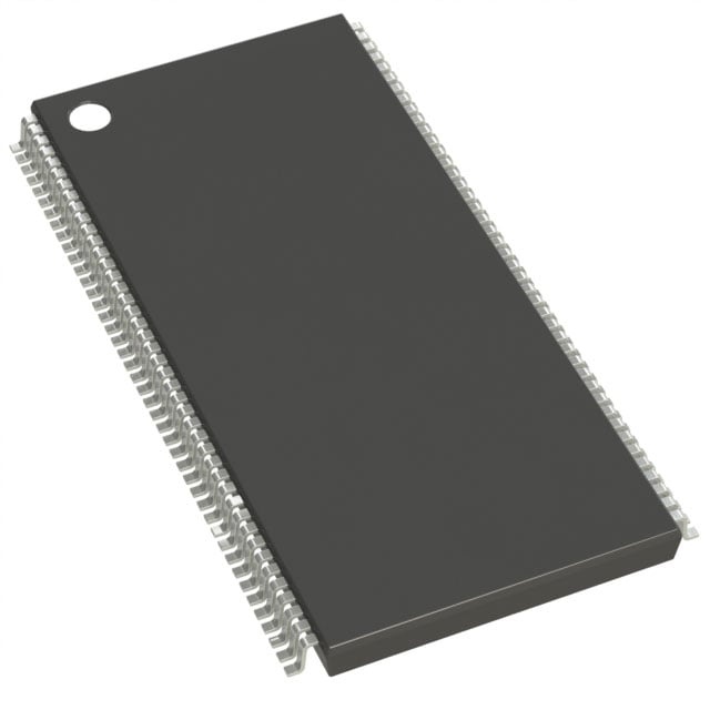
IS42S32200C1-7TL-TR
| Part Description |
IC DRAM 64MBIT PAR 86TSOP II |
|---|---|
| Quantity | 462 Available (as of June 15, 2026) |

| Product Category | Memory |
|---|---|
| Manufacturer | Integrated Silicon Solution Inc |
| Manufacturing Status | Obsolete |
| Manufacturer Standard Lead Time | Contact Us |
| Datasheet |
Specifications & Environmental
| Device Package | 86-TSOP II | Memory Format | DRAM | Technology | SDRAM | ||
|---|---|---|---|---|---|---|---|
| Memory Size | 64 Mbit | Access Time | 5.5 ns | Grade | Commercial | ||
| Clock Frequency | 143 MHz | Voltage | 3.15V ~ 3.45V | Memory Type | Volatile | ||
| Operating Temperature | 0°C ~ 70°C (TA) | Write Cycle Time Word Page | N/A | Packaging | 86-TFSOP (0.400", 10.16mm Width) | ||
| Mounting Method | Volatile | Memory Interface | Parallel | Memory Organization | 2M x 32 | ||
| Moisture Sensitivity Level | 3 (168 Hours) | RoHS Compliance | ROHS3 Compliant | REACH Compliance | REACH Unaffected | ||
| Qualification | N/A | ECCN | EAR99 | HTS Code | 8542.32.0002 |
Overview of IS42S32200C1-7TL-TR – IC DRAM 64MBIT PAR 86TSOP II
The IS42S32200C1-7TL-TR is a 64‑Mbit synchronous DRAM device organized as 2M × 32 with four internal banks. It implements a fully synchronous, pipelined architecture with LVTTL-compatible signals and a parallel memory interface, designed for 3.3 V memory systems.
This device suits designs that require burst-oriented high-speed SDRAM with programmable CAS latency and internal bank interleaving to hide row precharge, delivering predictable timing and refresh behavior for system memory applications.
Key Features
- Core / Memory Architecture — 64‑Mbit organization as 524,288 × 32 × 4 banks (2,048 rows × 256 columns × 32 bits per bank) enabling quad‑bank operation and bank interleaving.
- Performance — Clock frequency 143 MHz (part suffix -7) with programmable CAS latency (2 or 3 clocks) and access times down to 5.5 ns for CL=3.
- Interface — Fully synchronous operation with all inputs and outputs registered on the rising edge of CLK; LVTTL‑compatible I/O and parallel memory interface.
- Burst and Refresh — Programmable burst lengths (1, 2, 4, 8, full page) and selectable burst sequence (sequential/interleave); supports AUTO REFRESH and self‑refresh with 4096 refresh cycles every 64 ms.
- Power — Single 3.3 V power supply operation with specified voltage supply range of 3.15 V to 3.45 V and support for power‑down and self‑refresh modes.
- Timing — Random column address every clock cycle, burst read/write and burst read/single write capability, and burst termination via burst stop and precharge commands.
- Package — Offered in 86‑TSOP II (400‑mil, 10.16 mm width) package suitable for board‑level mounting; supplier device package: 86‑TSOP II.
- Operating Range — Specified operating ambient temperature range of 0°C to 70°C (TA).
Typical Applications
- 3.3 V Memory Subsystems — Use as parallel SDRAM memory in systems that require a 64‑Mbit synchronous DRAM device operating from a 3.3 V supply.
- High‑speed Burst Data Buffers — Suitable where programmable burst lengths and CAS latency are needed to tune throughput and latency for burst transfers.
- Board‑level Memory Expansion — Fits designs requiring an 86‑TSOP II package for board mounting and LVTTL interface compatibility.
Unique Advantages
- Quad‑bank organization: Internal 4‑bank layout enables bank interleaving to hide precharge time and improve sustained throughput during burst accesses.
- Flexible timing options: Programmable CAS latency (2 or 3 clocks) and multiple burst length/sequence settings allow timing optimization for different system requirements.
- Single‑rail power simplicity: Operates from a single 3.3 V supply (3.15–3.45 V), simplifying power‑rail design for compatible memory systems.
- Power management features: Self‑refresh and power‑down modes reduce standby power during idle periods.
- Standard package footprint: 86‑TSOP II (400‑mil, 10.16 mm) package supports common board designs for density and manufacturability.
Why Choose IC DRAM 64MBIT PAR 86TSOP II?
The IS42S32200C1-7TL-TR provides a compact, fully synchronous 64‑Mbit DRAM solution with programmable timing, burst control and internal bank architecture that help optimize performance for parallel memory systems running from a 3.3 V supply. Its LVTTL interface and TSOP II package make it suitable for board‑level memory implementations where predictable timing and refresh behavior are required.
This device is appropriate for designers who need a documented, quad‑bank SDRAM with configurable burst and CAS options to match system clocks and latency requirements. It is supported by full datasheet documentation from the manufacturer for integration and validation in production designs.
Request a quote or contact sales to discuss availability, pricing, and lead time for IS42S32200C1-7TL-TR.