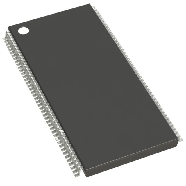
IS42S32200C1-7TL
| Part Description |
IC DRAM 64MBIT PAR 86TSOP II |
|---|---|
| Quantity | 607 Available (as of June 15, 2026) |

| Product Category | DRAM Memory |
|---|---|
| Manufacturer | Integrated Silicon Solution Inc |
| Manufacturing Status | Obsolete |
| Manufacturer Standard Lead Time | Contact Us |
| Datasheet |
Specifications & Environmental
| Device Package | 86-TSOP II | Memory Format | DRAM | Technology | SDRAM | ||
|---|---|---|---|---|---|---|---|
| Memory Size | 64 Mbit | Access Time | 5.5 ns | Grade | Commercial | ||
| Clock Frequency | 143 MHz | Voltage | 3.15V ~ 3.45V | Memory Type | Volatile | ||
| Operating Temperature | 0°C ~ 70°C (TA) | Write Cycle Time Word Page | N/A | Packaging | 86-TFSOP (0.400", 10.16mm Width) | ||
| Mounting Method | Volatile | Memory Interface | Parallel | Memory Organization | 2M x 32 | ||
| Moisture Sensitivity Level | 3 (168 Hours) | RoHS Compliance | ROHS Compliant | REACH Compliance | REACH Unaffected | ||
| Qualification | N/A | ECCN | EAR99 | HTS Code | 8542.32.0002 |
Overview of IS42S32200C1-7TL – IC DRAM 64MBIT PAR 86TSOP II
The IS42S32200C1-7TL is a 64‑Mbit synchronous DRAM (SDRAM) organized as 2M × 32 with four internal banks and a fully synchronous LVTTL interface. It is designed for 3.3V memory systems that require parallel SDRAM with programmable burst and latency options.
Its synchronous, pipeline architecture and quad-bank organization enable high‑speed burst transfers and bank interleaving to reduce access latency in systems using a 3.15–3.45V supply and operating across a 0°C to 70°C ambient range.
Key Features
- Core Architecture Quad‑bank SDRAM organized as 524,288 × 32 × 4 banks (each bank 16,777,216 bits) with pipeline architecture to support high‑speed synchronous operation.
- Memory Capacity & Organization 64 Mbit total capacity, internally configured as 2,048 rows × 256 columns × 32 bits per bank.
- Performance Speed grade -7 supports a clock frequency up to 143 MHz with CAS latency options and an access time as low as 5.5 ns (CAS‑3 timing shown for -7).
- Programmable Burst & CAS Programmable burst lengths (1, 2, 4, 8, full page) and burst sequences (Sequential/Interleave); programmable CAS latency of 2 or 3 clocks.
- Refresh & Power Modes Supports AUTO REFRESH, self refresh modes and requires 4096 refresh cycles every 64 ms for data integrity; single 3.3V power supply behavior (specified supply range 3.15V–3.45V).
- Interface LVTTL compatible inputs/outputs with all signals referenced to the rising edge of the clock (fully synchronous operation).
- Package 86‑pin TSOP II (400‑mil, 10.16 mm width) package suitable for parallel mounting in board‑level memory systems.
- Operating Range Commercial ambient operating temperature 0°C to 70°C (TA). The datasheet also notes availability in industrial temperature grades.
Typical Applications
- 3.3V Memory Subsystems Use as parallel SDRAM in systems that require a 64 Mbit synchronous DRAM device operating from a 3.15–3.45V supply.
- High‑speed Burst Data Buffers Suitable where programmable burst lengths, burst sequencing and CAS latency control are needed to match system timing.
- Bank‑interleaved Memory Designs Quad‑bank organization enables precharge hiding and interleaving strategies to improve random access throughput in parallel memory architectures.
Unique Advantages
- Flexible Timing Configuration: Programmable CAS latency (2 or 3 clocks) and multiple burst length/sequence options let designers tune throughput and latency to system needs.
- Quad‑Bank Architecture: Four internal banks allow bank interleaving and hidden precharge to reduce effective access times during random and burst operations.
- Synchronous LVTTL Interface: Fully synchronous operation referenced to the rising clock edge simplifies timing design for pipeline memory systems.
- Clear Refresh Management: Supports AUTO REFRESH and self‑refresh modes with 4096 refresh cycles every 64 ms, facilitating reliable data retention strategies.
- Industry‑standard Package: 86‑TSOP II (400‑mil) package provides a known board footprint for parallel SDRAM mounting and replacement.
Why Choose IS42S32200C1-7TL?
The IS42S32200C1-7TL delivers a compact 64‑Mbit synchronous DRAM solution with programmable timing, burst control and quad‑bank organization for designs that require predictable, high‑speed parallel memory behavior at 3.3V. Its LVTTL synchronous interface and support for multiple burst and CAS settings allow designers to optimize memory transactions for a variety of system timing requirements.
This device is well suited for engineers building 3.3V memory subsystems and board‑level designs that need a 64‑Mbit SDRAM in an 86‑pin TSOP II package, offering configurable performance and standard refresh/power modes to support reliable operation over the specified commercial temperature range.
Request a quote or contact sales to discuss availability, lead times and pricing for IS42S32200C1-7TL.