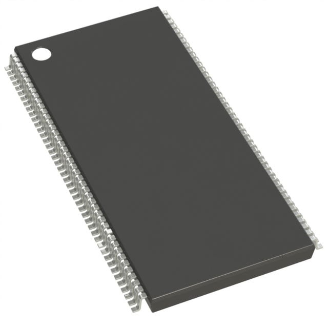
IS42S32200C1-7TLI-TR
| Part Description |
IC DRAM 64MBIT PAR 86TSOP II |
|---|---|
| Quantity | 483 Available (as of June 15, 2026) |

| Product Category | DRAM Memory |
|---|---|
| Manufacturer | Integrated Silicon Solution Inc |
| Manufacturing Status | Obsolete |
| Manufacturer Standard Lead Time | Contact Us |
| Datasheet |
Specifications & Environmental
| Device Package | 86-TSOP II | Memory Format | DRAM | Technology | SDRAM | ||
|---|---|---|---|---|---|---|---|
| Memory Size | 64 Mbit | Access Time | 5.5 ns | Grade | Industrial | ||
| Clock Frequency | 143 MHz | Voltage | 3.15V ~ 3.45V | Memory Type | Volatile | ||
| Operating Temperature | -40°C ~ 85°C (TA) | Write Cycle Time Word Page | N/A | Packaging | 86-TFSOP (0.400", 10.16mm Width) | ||
| Mounting Method | Volatile | Memory Interface | Parallel | Memory Organization | 2M x 32 | ||
| Moisture Sensitivity Level | 3 (168 Hours) | RoHS Compliance | ROHS3 Compliant | REACH Compliance | REACH Unaffected | ||
| Qualification | N/A | ECCN | EAR99 | HTS Code | 8542.32.0002 |
Overview of IS42S32200C1-7TLI-TR – IC DRAM 64MBIT PAR 86TSOP II
The IS42S32200C1-7TLI-TR is a 64‑Mbit synchronous dynamic RAM (SDRAM) organized as 524,288 × 32 × 4 banks. It is a fully synchronous, pipeline‑architecture DRAM designed for parallel memory interfaces and supports registered signals on the rising clock edge.
Key device characteristics include a single 3.3 V supply (3.15 V to 3.45 V), programmable burst lengths and sequences, LVTTL I/O, selectable CAS latency, and an industrial operating temperature range of -40°C to 85°C in an 86‑pin TSOP II package.
Key Features
- Memory Architecture and Capacity 64 Mbit total capacity, internally organized as 524,288 × 32 × 4 banks (4 banks × 16,777,216 bits each) for bank interleaving and improved throughput.
- Synchronous SDRAM Operation Fully synchronous operation with all inputs and outputs referenced to the rising clock edge; pipeline architecture enables high‑speed burst transfers.
- Performance Clock frequency up to 143 MHz for the -7 timing grade and access times down to 5.5 ns (CAS‑latency = 3). Programmable CAS latency options of 2 or 3 cycles.
- Burst and Access Control Programmable burst lengths (1, 2, 4, 8, full page) and selectable burst sequence (sequential or interleave). Supports burst read/write and burst read/single write modes with burst termination.
- Refresh and Power Modes Supports AUTO REFRESH and self‑refresh modes with 4096 refresh cycles every 64 ms, plus power‑down capabilities to reduce standby power.
- Interface and Signaling LVTTL compatible I/O and parallel memory interface for board‑level integration with 3.3 V systems.
- Package and Temperature Supplied in a 86‑pin TSOP II (400‑mil, 10.16 mm width) package; specified operating temperature range of -40°C to 85°C. Also available in a 90‑ball BGA option and in lead‑free variants per datasheet options.
Typical Applications
- High‑speed parallel memory subsystems — Used where a 64‑Mbit synchronous DRAM with burst capability and LVTTL interface is required for board‑level memory.
- Embedded systems requiring deterministic timing — Synchronous operation and programmable CAS latency provide predictable access characteristics for time‑sensitive designs.
- Industrial temperature designs — The -40°C to 85°C operating range supports deployments in temperature‑demanding environments.
- Legacy or replacement SDRAM modules — Pin‑compatible 86‑TSOP II packaging and standard 3.3 V supply make this suitable for module or board replacements where parallel SDRAM is used.
Unique Advantages
- Quad‑bank architecture for higher throughput: Four internal banks enable interleaving and hide precharge time to sustain continuous data transfers.
- Flexible burst and latency control: Programmable burst lengths and CAS latency (2 or 3) allow tuning for specific access patterns and system timing.
- Synchronous, pipeline timing: All signals registered on the rising clock edge for consistent, deterministic timing across reads and writes.
- Industrial‑grade temperature support: Specified from -40°C to 85°C for use in temperature‑challenging applications.
- Standard 86‑TSOP II packaging: 400‑mil TSOP II package (10.16 mm width) facilitates board‑level integration and common footprint usage.
- On‑die refresh and low‑power modes: AUTO REFRESH, self‑refresh, and power‑down modes help manage refresh requirements and reduce standby power.
Why Choose IS42S32200C1-7TLI-TR?
The IS42S32200C1-7TLI-TR provides a focused 64‑Mbit synchronous DRAM solution with programmable burst modes, selectable CAS latency, and a quad‑bank architecture to support sustained high‑speed parallel transfers. Its single 3.3 V supply, LVTTL interface, and TSOP II packaging make it suitable for designs that require straightforward integration into 3.3 V board environments.
This device is suitable for designers needing deterministic, synchronous memory with industrial temperature support and standard board‑level packaging. Sourcing the IS42S32200C1-7TLI-TR delivers a specification‑driven memory option from Integrated Silicon Solution, Inc., with datasheet‑documented timing, refresh, and packaging choices.
Request a quote or submit a quote request for IS42S32200C1-7TLI-TR through your preferred procurement channel to check availability, lead times, and pricing.