IS42S32200E-6B-TR
| Part Description |
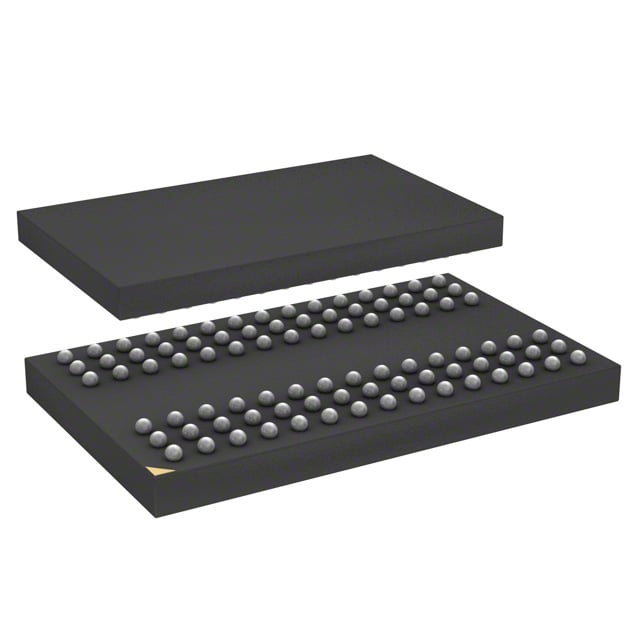
IC DRAM 64MBIT PARALLEL 90TFBGA |
|---|---|
| Quantity | 988 Available (as of June 15, 2026) |

| Product Category | Memory |
|---|---|
| Manufacturer | Integrated Silicon Solution Inc |
| Manufacturing Status | Obsolete |
| Manufacturer Standard Lead Time | Contact Us |
| Datasheet |
Specifications & Environmental
| Device Package | 90-TFBGA (8x13) | Memory Format | DRAM | Technology | SDRAM | ||
|---|---|---|---|---|---|---|---|
| Memory Size | 64 Mbit | Access Time | 5.5 ns | Grade | Commercial | ||
| Clock Frequency | 166 MHz | Voltage | 3V ~ 3.6V | Memory Type | Volatile | ||
| Operating Temperature | 0°C ~ 70°C (TA) | Write Cycle Time Word Page | N/A | Packaging | 90-TFBGA | ||
| Mounting Method | Volatile | Memory Interface | Parallel | Memory Organization | 2M x 32 | ||
| Moisture Sensitivity Level | 3 (168 Hours) | RoHS Compliance | ROHS3 Compliant | REACH Compliance | REACH Unaffected | ||
| Qualification | N/A | ECCN | EAR99 | HTS Code | 8542.32.0002 |
Overview of IS42S32200E-6B-TR – IC DRAM 64MBIT PARALLEL 90TFBGA
The IS42S32200E-6B-TR is a 64Mbit synchronous DRAM (SDRAM) device organized as 2M × 32 with a quad-bank architecture and a parallel memory interface. Designed for 3.3V system operation, this part provides synchronous, clock-referenced access and features programmable burst modes and selectable CAS latency for deterministic memory timing.
Key Features
- Core Architecture Quad-bank synchronous DRAM with all signals referenced to the rising edge of the clock; pipeline architecture enables synchronous operation and predictable timing.
- Memory Organization 64 Mbit capacity organized as 2M × 32, internally structured as four banks with each bank having 2,048 rows × 256 columns × 32 bits.
- Performance –6 grade supports a clock frequency of 166 MHz and an access time from clock of 5.5 ns (CAS latency = 3). Other device grades in the family support 200, 166, 143 and 133 MHz options.
- Interface & Control LVTTL-compatible control interface with programmable burst lengths (1, 2, 4, 8, full page), programmable burst sequence (sequential/interleave), and programmable CAS latency (2 or 3 clocks).
- Refresh & Power Single 3.3V supply operation; supports self-refresh modes and standard refresh cycles (examples in datasheet: 4096 refresh cycles per refresh period depending on grade).
- Operation & Timing Supports random column address every clock cycle, burst read/write and burst read/single write operations, and burst termination via burst stop and precharge commands.
- Package & Temperature Supplied in a 90‑TFBGA (8 × 13) package. Commercial operating temperature range documented as 0°C to +70°C (TA).
Typical Applications
- 3.3V system memory Use as parallel SDRAM in systems that require a 64 Mbit synchronous memory device with LVTTL control and programmable burst behavior.
- Buffered data storage Suitable where deterministic, clock-referenced burst reads/writes and selectable CAS latency are required for timing-critical buffering.
- Embedded memory subsystems Integrates into designs needing a compact 90‑TFBGA package and standard SDRAM refresh/self-refresh support.
Unique Advantages
- Quad‑bank organization: Enables internal bank operations to hide row access/precharge and improve effective throughput for burst operations.
- Programmable performance options: Selectable CAS latency (2 or 3) and burst lengths/sequences allow tuning for latency versus throughput needs.
- Standard 3.3V supply: Operates from a single 3.3V power rail (3.0V–3.6V specified), simplifying power design for legacy 3.3V platforms.
- Compact BGA package: 90‑TFBGA (8×13) package supports high-density board implementations while providing the required I/O footprint.
- Synchronous, clocked operation: All inputs/outputs referenced to the positive clock edge for predictable timing and integration with synchronous system buses.
Why Choose IS42S32200E-6B-TR?
The IS42S32200E-6B-TR delivers a deterministic, synchronous 64Mbit DRAM solution with programmable timing and burst flexibility for designs that require a 3.3V parallel memory interface. Its quad-bank architecture, selectable CAS latency, and support for burst read/write modes make it suitable for systems needing predictable memory timing and efficient burst data transfers.
This device is appropriate for designers seeking a compact 90‑TFBGA packaged SDRAM with documented timing parameters (166 MHz clock grade, 5.5 ns access from clock at CL=3) and standard refresh/self-refresh capabilities as specified in the datasheet.
Request a quote or submit an inquiry for pricing and availability to receive lead-time and quantity information for the IS42S32200E-6B-TR.