IS42S32200E-6BI-TR
| Part Description |
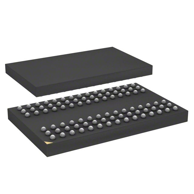
IC DRAM 64MBIT PARALLEL 90TFBGA |
|---|---|
| Quantity | 875 Available (as of June 14, 2026) |

| Product Category | Memory |
|---|---|
| Manufacturer | Integrated Silicon Solution Inc |
| Manufacturing Status | Obsolete |
| Manufacturer Standard Lead Time | Contact Us |
| Datasheet |
Specifications & Environmental
| Device Package | 90-TFBGA (8x13) | Memory Format | DRAM | Technology | SDRAM | ||
|---|---|---|---|---|---|---|---|
| Memory Size | 64 Mbit | Access Time | 5.5 ns | Grade | Industrial | ||
| Clock Frequency | 166 MHz | Voltage | 3V ~ 3.6V | Memory Type | Volatile | ||
| Operating Temperature | -40°C ~ 85°C (TA) | Write Cycle Time Word Page | N/A | Packaging | 90-TFBGA | ||
| Mounting Method | Volatile | Memory Interface | Parallel | Memory Organization | 2M x 32 | ||
| Moisture Sensitivity Level | 3 (168 Hours) | RoHS Compliance | ROHS3 Compliant | REACH Compliance | REACH Unaffected | ||
| Qualification | N/A | ECCN | EAR99 | HTS Code | 8542.32.0002 |
Overview of IS42S32200E-6BI-TR – IC DRAM 64MBIT PARALLEL 90TFBGA
The IS42S32200E-6BI-TR is a 64 Mbit synchronous DRAM device organized for high-speed parallel memory applications. It implements a synchronous, pipelined architecture with internal bank management and a parallel LVTTL interface for deterministic, clock-referenced data transfers.
Designed to operate from a 3.3 V supply (3.0 V to 3.6 V) and specified for an operating ambient range of -40°C to 85°C, this device targets 3.3 V memory systems requiring a compact 90‑TFBGA package and flexible burst and timing options.
Key Features
- Memory Capacity & Organization — 64 Mbit total capacity with organization listed as 2M × 32 and internal quad-bank architecture to hide row access/precharge and improve throughput.
- High‑speed Synchronous Operation — Speed grade -6 providing a clock frequency of 166 MHz and an access time from clock of 5.5 ns (CAS latency = 3).
- Programmable Burst & Timing — Programmable burst length (1, 2, 4, 8, full page) and programmable burst sequence (sequential/interleave); selectable CAS latency (2 or 3 clocks).
- Refresh & Self‑Refresh Support — Supports auto-refresh and self-refresh modes with 4096 refresh cycles and timing options that vary by device grade (e.g., 16 ms or 64 ms refresh windows noted in the device specification).
- Power & I/O — Single 3.3 V power supply operation with LVTTL-compatible interface for control and data signaling.
- Package — 90‑TFBGA (8 × 13) ball grid array for space-efficient mounting.
- Temperature Range — Specified operating ambient temperature of -40°C to 85°C (TA).
Typical Applications
- 3.3 V Memory Systems — Designed to operate within 3.3 V memory subsystems requiring 64 Mbit synchronous DRAM capacity.
- High‑speed Data Transfer Modules — Pipeline architecture and synchronous clocked operation enable high-speed, clock-referenced transfers in parallel memory designs.
- Compact, Board‑Level Memory — 90‑TFBGA package provides a space-efficient footprint for board-level memory implementations that require a parallel LVTTL interface.
Unique Advantages
- Flexible Timing Options: CAS latency selectable between 2 and 3 clocks and multiple speed grades available; -6 speed grade offers 166 MHz clock operation.
- Programmable Burst Control: Multiple burst lengths and sequence modes enable optimized read/write patterns for system memory access behavior.
- Quad‑Bank Architecture: Four internal banks help hide row access/precharge cycles to improve sustained throughput.
- Narrow Voltage Range Support: Operates from 3.0 V to 3.6 V, matching standard 3.3 V memory system designs.
- Industry‑Level Temperature Spec: Rated for -40°C to 85°C ambient operation for deployments needing extended temperature tolerance.
- Space‑Efficient Package: 90‑ball TF‑BGA (8×13) package balances density and board mounting for compact designs.
Why Choose IC DRAM 64MBIT PARALLEL 90TFBGA?
The IS42S32200E-6BI-TR provides a synchronous, high-speed 64 Mbit DRAM solution with configurable burst modes, selectable CAS latencies, and an internal quad‑bank architecture that supports efficient parallel memory access. Its 166 MHz speed grade, 5.5 ns access time (CL=3), and LVTTL interface make it suitable for 3.3 V memory systems where predictable, clocked transfers are required.
With a compact 90‑TFBGA package and an operating ambient range down to -40°C, this device is appropriate for designs that require a balance of performance, board density, and extended temperature capability while operating from a standard 3.3 V supply.
To request a quote or submit an inquiry for IS42S32200E-6BI-TR, please contact our sales team with your part quantity and delivery requirements.