IS42S32200E-6BLI
| Part Description |
IC DRAM 64MBIT PARALLEL 90TFBGA |
|---|---|
| Quantity | 1,216 Available (as of June 15, 2026) |
| Product Category | Memory |
|---|---|
| Manufacturer | Integrated Silicon Solution Inc |
| Manufacturing Status | Obsolete |
| Manufacturer Standard Lead Time | Contact Us |
| Datasheet |
Specifications & Environmental
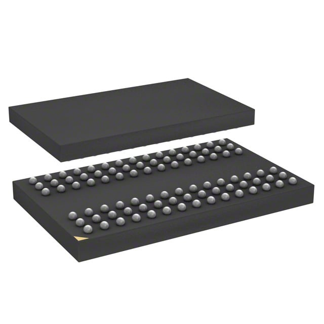
| Device Package | 90-TFBGA (8x13) | Memory Format | DRAM | Technology | SDRAM | ||
|---|---|---|---|---|---|---|---|
| Memory Size | 64 Mbit | Access Time | 5.5 ns | Grade | Industrial | ||
| Clock Frequency | 166 MHz | Voltage | 3V ~ 3.6V | Memory Type | Volatile | ||
| Operating Temperature | -40°C ~ 85°C (TA) | Write Cycle Time Word Page | N/A | Packaging | 90-TFBGA | ||
| Mounting Method | Volatile | Memory Interface | Parallel | Memory Organization | 2M x 32 | ||
| Moisture Sensitivity Level | 3 (168 Hours) | RoHS Compliance | ROHS Compliant | REACH Compliance | REACH Unaffected | ||
| Qualification | N/A | ECCN | EAR99 | HTS Code | 8542.32.0002 |
Overview of IS42S32200E-6BLI – IC DRAM 64MBIT PARALLEL 90TFBGA
The IS42S32200E-6BLI is a 64 Mbit synchronous DRAM (SDRAM) device organized as 2M × 32 with a quad-bank architecture and pipeline operation. It is designed for 3.3 V memory systems, providing a parallel LVTTL interface and programmable timing to support a range of synchronous memory subsystems.
Targeted at designs requiring synchronous parallel DRAM, the device offers a 166 MHz clock option, programmable burst modes, and a compact 90‑TFBGA package with an operating temperature range of −40°C to +85°C.
Key Features
- Core Architecture Quad-bank SDRAM organization with internal bank management to hide row access and precharge operations; memory organized as 2M × 32 for a total of 64 Mbit.
- Memory Performance Synchronous SDRAM rated for a 166 MHz clock frequency (–6 option) with an access time of 5.5 ns (CAS latency = 3).
- Burst and Sequencing Programmable burst lengths (1, 2, 4, 8, full page) and selectable sequential or interleave burst sequences; supports burst read/write and burst read/single write operations with burst termination commands.
- Timing Flexibility Programmable CAS latency options (2 or 3 clocks) and random column addressing every clock cycle to accommodate different system timing requirements.
- Power and Interface Single 3.3 V supply operation (3.0 V to 3.6 V range) with LVTTL-compatible interface signals.
- Refresh and Self-Refresh Auto refresh and self-refresh modes supported; specified refresh cycles include 4096 refresh cycles per 16 ms or 64 ms depending on device grade.
- Package and Temperature Supplied in a 90‑ball TF‑BGA (90‑TFBGA, 8×13) package and specified for an operating temperature range of −40°C to +85°C (TA).
Typical Applications
- 3.3 V synchronous memory subsystems — Deploy as parallel SDRAM in systems designed around a 3.3 V memory rail with LVTTL signaling.
- High-speed parallel data buffering — Use where a 166 MHz synchronous interface and programmable burst operation are required for short-latency transfers.
- Industrial and temperature-sensitive systems — Suitable for designs that require operation across −40°C to +85°C.
- Embedded systems with LVTTL interface — Integrate where a parallel SDRAM with flexible timing and refresh control is needed.
Unique Advantages
- Deterministic synchronous interface: All signals referenced to the rising clock edge simplifies timing analysis and system integration.
- Flexible performance tuning: Programmable CAS latency and multiple burst length/sequence options let designers optimize throughput and latency trade-offs.
- Compact BGA footprint: 90‑TFBGA (8×13) package minimizes board area while delivering 64 Mbit density.
- Single-supply operation: 3.0–3.6 V supply range supports standard 3.3 V memory rails for straightforward power provisioning.
- Built-in refresh management: Auto and self-refresh modes plus defined refresh-cycle options reduce external refresh management complexity.
- High-frequency option: 166 MHz rating with 5.5 ns access time (CAS = 3) offers a high-speed option within the IS42S32200E family.
Why Choose IS42S32200E-6BLI?
The IS42S32200E-6BLI combines 64 Mbit SDRAM density with a synchronous, quad-bank architecture and flexible timing controls to suit designs that need predictable, high-speed parallel memory. Its single 3.3 V supply, LVTTL interface, programmable burst and CAS options, and compact 90‑TFBGA package make it well suited for memory subsystems where board space and timing flexibility are important.
This device fits designers and system integrators building 3.3 V synchronous memory systems that require defined refresh behavior and an operating range to −40°C to +85°C, delivering a stable, specification-driven memory option for mid-density SDRAM needs.
Request a quote or submit a request for pricing and lead-time information to receive availability and procurement details for the IS42S32200E-6BLI.