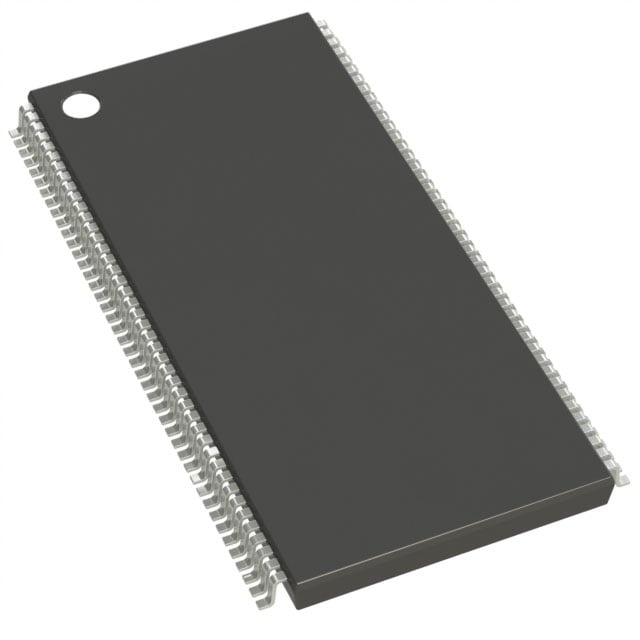
IS42S32200E-6TL
| Part Description |
IC DRAM 64MBIT PAR 86TSOP II |
|---|---|
| Quantity | 1,345 Available (as of June 15, 2026) |
| Product Category | Memory |
|---|---|
| Manufacturer | Integrated Silicon Solution Inc |
| Manufacturing Status | Obsolete |
| Manufacturer Standard Lead Time | Contact Us |
| Datasheet |
Specifications & Environmental
| Device Package | 86-TSOP II | Memory Format | DRAM | Technology | SDRAM | ||
|---|---|---|---|---|---|---|---|
| Memory Size | 64 Mbit | Access Time | 5.5 ns | Grade | Commercial | ||
| Clock Frequency | 166 MHz | Voltage | 3V ~ 3.6V | Memory Type | Volatile | ||
| Operating Temperature | 0°C ~ 70°C (TA) | Write Cycle Time Word Page | N/A | Packaging | 86-TFSOP (0.400", 10.16mm Width) | ||
| Mounting Method | Volatile | Memory Interface | Parallel | Memory Organization | 2M x 32 | ||
| Moisture Sensitivity Level | 3 (168 Hours) | RoHS Compliance | ROHS3 Compliant | REACH Compliance | REACH Unaffected | ||
| Qualification | N/A | ECCN | EAR99 | HTS Code | 8542.32.0002 |
Overview of IS42S32200E-6TL – IC DRAM 64MBIT PAR 86TSOP II
The IS42S32200E-6TL is a 64‑Mbit synchronous DRAM (SDRAM) device organized as 2M × 32 with four internal banks. It implements a fully synchronous, pipelined architecture with all signals referenced to the rising edge of the clock.
Designed for 3.3V memory systems requiring a parallel SDRAM interface, this device delivers predictable, clocked memory access with programmable burst modes and selectable CAS latency for system memory buffering and high‑throughput data transfers.
Key Features
- Core Architecture Quad‑bank SDRAM organization (4 banks) enabling internal bank operations to hide row access/precharge and improve throughput.
- Memory Capacity & Organization 64 Mbit total capacity organized as 2M × 32 bits, suitable for parallel memory subsystems requiring 32‑bit data paths.
- Clock & Timing 166 MHz clock frequency (‑6 speed grade) with programmable CAS latency (2 or 3 clocks) and typical access time from clock of 5.5 ns (CAS latency = 3).
- Burst Control Programmable burst lengths (1, 2, 4, 8, full page) and selectable burst sequence (sequential or interleave) for flexible read/write burst behavior.
- Interface & Logic Levels LVTTL compatible interface with fully synchronous control referenced to the positive clock edge for predictable timing integration.
- Power Single 3.3 V power supply support; specified supply range 3.0 V to 3.6 V.
- Refresh & Low‑Power Modes Supports self‑refresh and auto refresh modes. Datasheet options include 4,096 refresh cycles per 16 ms (A2 grade) or per 64 ms for commercial/A1 grades.
- Package & Temperature Available in 86‑pin TSOP II (86‑TFSOP, 0.400" / 10.16 mm width) package; commercial operating temperature 0°C to +70°C (TA).
Typical Applications
- Parallel Memory Subsystems Acts as a 32‑bit parallel SDRAM device for systems that require clocked, burstable memory buffers.
- System Buffers and Frame Stores Provides burst read/write capability and random column access every clock cycle for temporary data buffering in memory‑intensive designs.
- 3.3V Digital Platforms Suited to digital systems designed around a single 3.3 V supply and LVTTL memory interfaces.
Unique Advantages
- Quad‑Bank Architecture: Four internal banks reduce effective row access latency by allowing bank interleaving and overlap of operations.
- Programmable Burst and CAS Settings: Configurable burst lengths, sequences, and CAS latency let designers tune throughput and latency for application needs.
- Clocked, Predictable Operation: Fully synchronous operation referenced to the rising clock edge simplifies timing analysis and system integration.
- Narrow TSOP II Footprint: 86‑pin TSOP II package (0.400", 10.16 mm width) offers a compact form factor for board space‑constrained designs.
- Refresh and Self‑Refresh Support: Multiple refresh modes supported to maintain data integrity with options matching commercial and A‑grade refresh intervals.
- Wide Supply Tolerance: Operates across a 3.0 V to 3.6 V supply range while targeting a single 3.3 V power rail.
Why Choose IC DRAM 64MBIT PAR 86TSOP II?
The IS42S32200E-6TL positions itself as a compact, fully synchronous 64 Mbit SDRAM option for designs that require a 32‑bit parallel memory interface, programmable burst operation, and predictable clocked timing. Its quad‑bank organization and selectable CAS latency provide flexibility for memory subsystems where throughput and latency tradeoffs must be balanced.
This device is appropriate for designers building 3.3 V parallel memory systems who need a standardized TSOP II package with commercial‑grade temperature specification and documented refresh and timing options. The combination of programmable burst modes, LVTTL interface, and a defined 166 MHz speed grade simplifies integration into existing parallel memory architectures.
Request a quote or contact sales to discuss pricing, availability, or to submit a sourcing inquiry for IS42S32200E-6TL.