IS42S32200E-6TLI-TR
| Part Description |
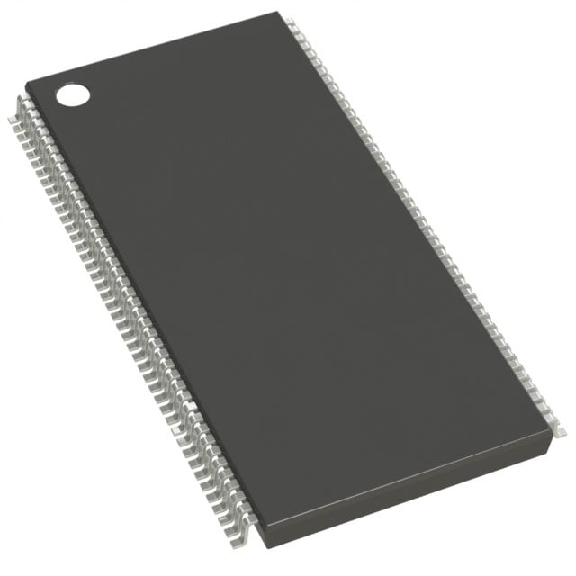
IC DRAM 64MBIT PAR 86TSOP II |
|---|---|
| Quantity | 1,307 Available (as of June 10, 2026) |

| Product Category | Memory |
|---|---|
| Manufacturer | Integrated Silicon Solution Inc |
| Manufacturing Status | Obsolete |
| Manufacturer Standard Lead Time | Contact Us |
| Datasheet |
Specifications & Environmental
| Device Package | 86-TSOP II | Memory Format | DRAM | Technology | SDRAM | ||
|---|---|---|---|---|---|---|---|
| Memory Size | 64 Mbit | Access Time | 5.5 ns | Grade | Industrial | ||
| Clock Frequency | 166 MHz | Voltage | 3V ~ 3.6V | Memory Type | Volatile | ||
| Operating Temperature | -40°C ~ 85°C (TA) | Write Cycle Time Word Page | N/A | Packaging | 86-TFSOP (0.400", 10.16mm Width) | ||
| Mounting Method | Volatile | Memory Interface | Parallel | Memory Organization | 2M x 32 | ||
| Moisture Sensitivity Level | 3 (168 Hours) | RoHS Compliance | ROHS3 Compliant | REACH Compliance | REACH Unaffected | ||
| Qualification | N/A | ECCN | EAR99 | HTS Code | 8542.32.0002 |
Overview of IS42S32200E-6TLI-TR – IC DRAM 64MBIT PAR 86TSOP II
The IS42S32200E-6TLI-TR is a 64 Mbit synchronous DRAM organized as 524,288 × 32 × 4 banks, designed for 3.3 V memory systems. It uses a pipelined, fully synchronous architecture with all signals referenced to the rising clock edge for deterministic timing in parallel memory designs.
Targeted at systems requiring board-level DRAM capacity and predictable performance, this device delivers selectable burst operations, programmable CAS latency, self-refresh and internal banking to optimize throughput and memory efficiency within a 86‑TSOP II package.
Key Features
- Memory Architecture – 64 Mbit capacity organized as 524,288 × 32 × 4 banks (2M × 32) for banked access and improved concurrency.
- Synchronous Operation – Fully synchronous DRAM with all inputs/outputs referenced to a positive clock edge and pipeline architecture for predictable timing.
- Performance – Supports a 166 MHz clock frequency (part -6) with access time of 5.5 ns (CAS latency = 3).
- Programmable Burst and CAS – Programmable burst lengths (1, 2, 4, 8, full page) and burst sequences (sequential/interleave); CAS latency programmable to 2 or 3 clocks.
- Refresh and Power – Supports self-refresh and AUTO REFRESH modes with 4096 refresh cycles per interval options; single 3.3 V supply operation (voltage range 3.0 V–3.6 V).
- Interface – Parallel memory interface with LVTTL signaling and ability to perform random column access every clock cycle.
- Package and Temperature – 86‑pin TSOP‑II package (10.16 mm width) and specified operating temperature range of -40 °C to +85 °C (TA).
Typical Applications
- 3.3 V Memory Subsystems – Board-level DRAM expansion in systems designed for a single 3.3 V supply and LVTTL interface.
- Embedded Systems – Use where synchronous, pipelined DRAM and programmable burst operations are required for predictable memory performance.
- Industrial Electronics – Suitable for applications requiring operation across -40 °C to +85 °C ambient temperature ranges.
- Legacy Parallel Memory Designs – Drop-in replacement or upgrade for parallel SDRAM designs using a TSOP‑II footprint.
Unique Advantages
- Quad‑Bank Organization: Internal four‑bank structure hides row access and precharge latency to improve effective throughput.
- Programmable Timing and Burst Control: Selectable CAS latency and burst length/sequence options allow designers to tune latency versus throughput for specific workloads.
- Deterministic Synchronous Interface: Fully synchronous operation with LVTTL signaling and pipelined architecture simplifies timing analysis and system integration.
- Industrial Temperature Range: Specified for -40 °C to +85 °C operation to meet extended environmental requirements.
- Standard TSOP‑II Package: 86‑pin TSOP‑II (10.16 mm width) enables compact board-level implementation in established footprints.
- Single Supply Operation: Designed for 3.3 V systems with a supply tolerance of 3.0 V–3.6 V for straightforward power integration.
Why Choose IS42S32200E-6TLI-TR?
The IS42S32200E-6TLI-TR offers a synchronous, pipelined 64 Mbit DRAM solution with programmable latency, burst control and internal banking to balance latency and throughput in parallel memory architectures. Its 166 MHz capability (part -6), 5.5 ns access timing at CAS‑3, and LVTTL interface provide predictable performance for board-level memory subsystems.
This device is suited for designs that require a compact TSOP‑II footprint, single 3.3 V supply operation, and extended temperature operation to -40 °C. It provides designers with configurable timing and refresh options to align memory behavior with application requirements while maintaining a standard package for straightforward integration.
Request a quote or submit an inquiry to discuss availability, lead times and pricing for IS42S32200E-6TLI-TR.