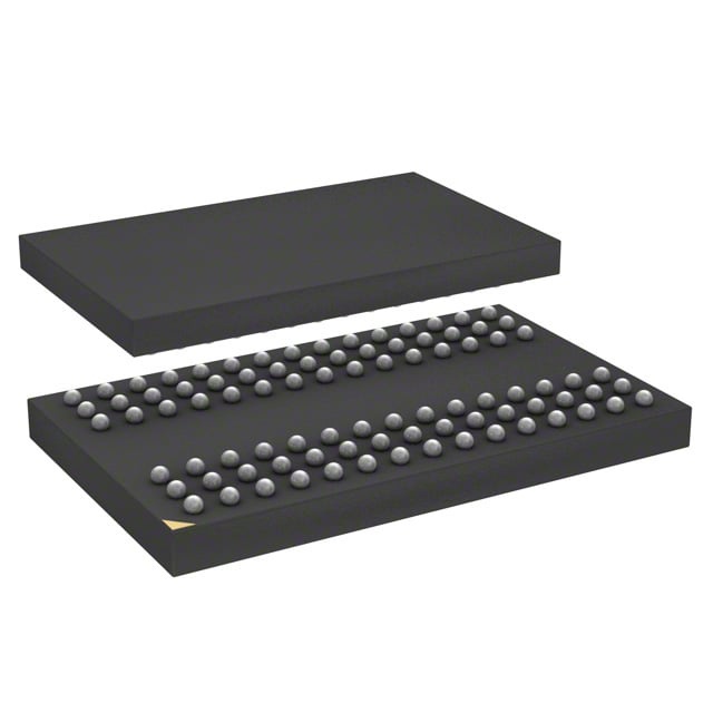
IS42S32200E-7BLI
| Part Description |
IC DRAM 64MBIT PAR 90TFBGA |
|---|---|
| Quantity | 101 Available (as of June 15, 2026) |

| Product Category | Memory |
|---|---|
| Manufacturer | Integrated Silicon Solution Inc |
| Manufacturing Status | Obsolete |
| Manufacturer Standard Lead Time | Contact Us |
| Datasheet |
Specifications & Environmental
| Device Package | 90-TFBGA (8x13) | Memory Format | DRAM | Technology | SDRAM | ||
|---|---|---|---|---|---|---|---|
| Memory Size | 64 Mbit | Access Time | 5.5 ns | Grade | Industrial | ||
| Clock Frequency | 143 MHz | Voltage | 3V ~ 3.6V | Memory Type | Volatile | ||
| Operating Temperature | -40°C ~ 85°C (TA) | Write Cycle Time Word Page | N/A | Packaging | 90-TFBGA | ||
| Mounting Method | Volatile | Memory Interface | Parallel | Memory Organization | 2M x 32 | ||
| Moisture Sensitivity Level | 3 (168 Hours) | RoHS Compliance | ROHS3 Compliant | REACH Compliance | REACH Unaffected | ||
| Qualification | N/A | ECCN | EAR99 | HTS Code | 8542.32.0002 |
Overview of IS42S32200E-7BLI – IC DRAM 64MBIT PAR 90TFBGA
The IS42S32200E-7BLI is a 64‑Mbit synchronous DRAM (SDRAM) from Integrated Silicon Solution Inc., organized as 2M × 32 with internal 4‑bank architecture. It provides a fully synchronous, pipelined interface for parallel memory applications that require deterministic timing and high‑speed data transfer.
Designed for 3.3 V systems (operating range 3.0 V–3.6 V) and specified for industrial temperature operation (−40°C to +85°C), this device targets designs that need a compact 90‑TFBGA package footprint with programmable latency and burst capabilities.
Key Features
- Core / Architecture Quad‑bank SDRAM architecture with internal bank management to hide row access and precharge latencies.
- Memory Organization & Capacity 64 Mbit total capacity organized as 2M × 32 (524,288 × 32 × 4 banks).
- Performance Supports clock frequencies up to 143 MHz for this device grade, with access time from clock of 5.5 ns (CAS latency = 3) and programmable CAS latency (2 or 3 clocks).
- Burst & Sequencing Programmable burst length (1, 2, 4, 8, full page) and selectable burst sequence (sequential/interleave) with burst termination options.
- Refresh & Self‑Refresh Supports AUTO REFRESH and self‑refresh modes with specified refresh cycle requirements (4096 cycles per refresh interval per datasheet grades).
- Interface & Signalling Fully synchronous interface with LVTTL signaling; all inputs and outputs are referenced to the rising edge of the clock.
- Power Single 3.3 V power supply operation (specified supply range 3.0 V–3.6 V).
- Package & Temperature 90‑ball TF‑BGA (90‑TFBGA, 8×13) supplier device package; operating temperature −40°C to +85°C (TA).
Typical Applications
- Parallel memory subsystems — Use as synchronous parallel DRAM in designs requiring a 64 Mbit footprint and 32‑bit data paths.
- Industrial temperature designs — Suitable for systems that require operation across −40°C to +85°C while maintaining 3.3 V supply compatibility.
- High‑speed buffering — Employed where burst read/write and programmable CAS latency at 143 MHz-class clocks are needed for predictable data throughput.
- Synchronous bus architectures — Fits applications that depend on clock‑referenced signaling and LVTTL interface timing.
Unique Advantages
- Programmable latency and bursts: CAS latency selectable (2 or 3 clocks) and flexible burst lengths let designers tune performance to system timing requirements.
- Quad‑bank hidden‑access architecture: Internal bank structure reduces effective row access/precharge overhead for improved sustained throughput.
- Industrial temperature range: Specified operation from −40°C to +85°C supports deployments in temperature‑challenging environments.
- Single‑supply 3.3 V operation: Simplifies power rail design while supporting a 3.0 V–3.6 V supply window for system tolerance.
- Compact TF‑BGA footprint: 90‑ball TFBGA (8×13) package minimizes PCB area for space‑constrained assemblies.
Why Choose IS42S32200E-7BLI?
The IS42S32200E-7BLI delivers a practical balance of density, timing flexibility, and industrial temperature capability in a compact 90‑TFBGA package. Its fully synchronous, pipelined design with programmable burst and CAS options makes it suitable for systems that require predictable, clock‑referenced memory behavior at 143 MHz device grade performance.
This SDRAM is well suited to designs that need a 64‑Mbit parallel memory solution with single‑supply 3.3 V operation and a −40°C to +85°C operating window, offering deterministic timing and integration into existing parallel memory interfaces.
Request a quote or submit an inquiry to discuss availability, lead times, and pricing for the IS42S32200E-7BLI.