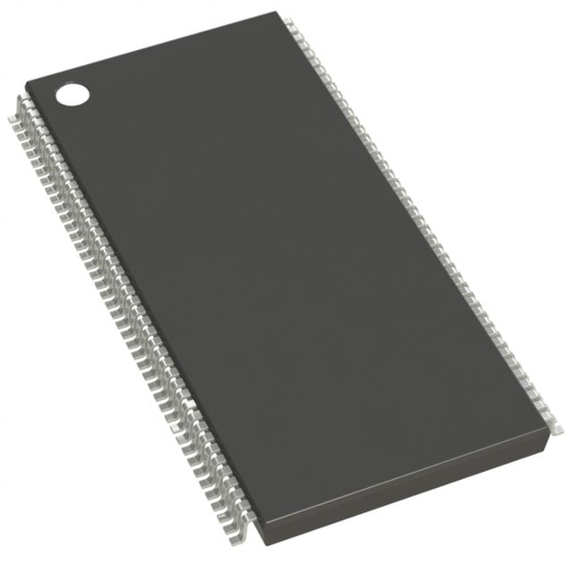
IS42S32200E-7TLI
| Part Description |
IC DRAM 64MBIT PAR 86TSOP II |
|---|---|
| Quantity | 793 Available (as of June 14, 2026) |

| Product Category | Memory |
|---|---|
| Manufacturer | Integrated Silicon Solution Inc |
| Manufacturing Status | Obsolete |
| Manufacturer Standard Lead Time | Contact Us |
| Datasheet |
Specifications & Environmental
| Device Package | 86-TSOP II | Memory Format | DRAM | Technology | SDRAM | ||
|---|---|---|---|---|---|---|---|
| Memory Size | 64 Mbit | Access Time | 5.5 ns | Grade | Industrial | ||
| Clock Frequency | 143 MHz | Voltage | 3V ~ 3.6V | Memory Type | Volatile | ||
| Operating Temperature | -40°C ~ 85°C (TA) | Write Cycle Time Word Page | N/A | Packaging | 86-TFSOP (0.400", 10.16mm Width) | ||
| Mounting Method | Volatile | Memory Interface | Parallel | Memory Organization | 2M x 32 | ||
| Moisture Sensitivity Level | 3 (168 Hours) | RoHS Compliance | ROHS3 Compliant | REACH Compliance | REACH Unaffected | ||
| Qualification | N/A | ECCN | EAR99 | HTS Code | 8542.32.0002 |
Overview of IS42S32200E-7TLI – IC DRAM 64Mbit 86‑TSOP II
The IS42S32200E-7TLI is a 64‑Mbit synchronous DRAM (SDRAM) device organized as 2M × 32 with a quad‑bank, pipelined architecture. It provides a parallel memory interface and LVTTL signaling for use in 3.3V memory systems.
Designed for high‑speed, synchronous memory applications, this device serves embedded and industrial designs that require predictable timing, programmable burst access, and extended temperature operation to −40°C to +85°C.
Key Features
- Core & architecture 64‑Mbit SDRAM organized as 2M × 32 with a 4‑bank, pipelined architecture and fully synchronous operation referenced to the positive clock edge.
- Performance Supports clock frequencies up to 143 MHz (device timing option), with an access time of 5.5 ns and programmable CAS latency (2 or 3 clocks).
- Memory & burst control Programmable burst lengths (1, 2, 4, 8, full page) and programmable burst sequence (sequential/interleave); burst read/write and burst read/single write capabilities with burst termination commands.
- Interface Parallel memory interface with LVTTL signaling and random column address capability every clock cycle for sustained throughput.
- Power Single 3.3 V power supply with specified operating range of 3.0 V to 3.6 V.
- Refresh & low‑power modes Auto refresh and self‑refresh support; refresh cycle options include 4096 cycles per 16 ms (A2 grade) or 4096 cycles per 64 ms (Commercial/Industrial/A1 grades) as documented.
- Package & temperature Available in an 86‑pin TSOP‑II (86‑TFSOP, 0.400", 10.16 mm width) package and specified for operation from −40°C to +85°C (TA).
Typical Applications
- Embedded system memory Provides synchronous 64‑Mbit DRAM for embedded platforms that use parallel SDRAM and 3.3 V supply rails.
- Industrial control Suitable for control and automation hardware that require extended temperature range and deterministic memory timing.
- Data buffering and temporary storage Used where high‑speed burst transfers and random column access every clock cycle are required for buffering or intermediate data storage.
Unique Advantages
- Synchronous pipelined design: Enables predictable timing and high throughput by referencing all signals to the positive clock edge.
- Flexible burst configuration: Programmable burst lengths and sequences let designers optimize memory transfers for specific access patterns.
- Wide voltage tolerance: Operates across 3.0 V to 3.6 V, aligning with common 3.3 V system supplies.
- Extended temperature rating: Specified operation from −40°C to +85°C for deployments in thermally demanding environments.
- Compact TSOP‑II package: 86‑pin TSOP‑II (10.16 mm width) simplifies PCB layout in space‑constrained designs.
- Refresh and low‑power support: Auto‑refresh and self‑refresh modes support system reliability and power management strategies.
Why Choose IC DRAM 64MBIT PAR 86TSOP II?
The IS42S32200E-7TLI delivers a compact, synchronous 64‑Mbit DRAM solution with programmable burst control, LVTTL interface, and a 4‑bank pipelined architecture for predictable, high‑speed memory access. Its 3.0–3.6 V supply range and −40°C to +85°C operating window make it appropriate for embedded and industrial designs that require reliable, parallel SDRAM operation.
This device is well suited to designers seeking a proven SDRAM building block with configurable timing (CAS latency and burst modes), standard refresh options, and a space‑efficient 86‑pin TSOP‑II package to simplify integration into legacy or new 3.3 V memory subsystems.
Request a quote or submit an RFQ to check current availability and pricing for IS42S32200E-7TLI.