IS42S32200E-7TL-TR
| Part Description |
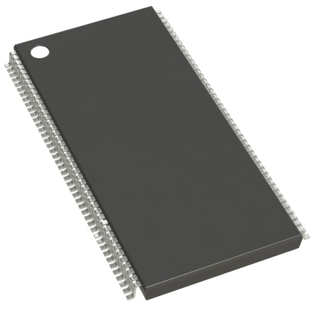
IC DRAM 64MBIT PAR 86TSOP II |
|---|---|
| Quantity | 671 Available (as of June 10, 2026) |

| Product Category | Memory |
|---|---|
| Manufacturer | Integrated Silicon Solution Inc |
| Manufacturing Status | Obsolete |
| Manufacturer Standard Lead Time | Contact Us |
| Datasheet |
Specifications & Environmental
| Device Package | 86-TSOP II | Memory Format | DRAM | Technology | SDRAM | ||
|---|---|---|---|---|---|---|---|
| Memory Size | 64 Mbit | Access Time | 5.5 ns | Grade | Commercial | ||
| Clock Frequency | 143 MHz | Voltage | 3V ~ 3.6V | Memory Type | Volatile | ||
| Operating Temperature | 0°C ~ 70°C (TA) | Write Cycle Time Word Page | N/A | Packaging | 86-TFSOP (0.400", 10.16mm Width) | ||
| Mounting Method | Volatile | Memory Interface | Parallel | Memory Organization | 2M x 32 | ||
| Moisture Sensitivity Level | 3 (168 Hours) | RoHS Compliance | ROHS Compliant | REACH Compliance | REACH Unaffected | ||
| Qualification | N/A | ECCN | EAR99 | HTS Code | 8542.32.0002 |
Overview of IS42S32200E-7TL-TR – IC DRAM 64MBIT PAR 86TSOP II
The IS42S32200E-7TL-TR is a 64 Mbit synchronous DRAM (SDRAM) device from ISSI, organized as 2M × 32 with four internal banks for improved throughput. Designed for 3.3 V memory systems and a parallel LVTTL interface, this part targets applications that require synchronous, high-speed volatile storage with programmable burst and latency options within a commercial 0°C to +70°C operating temperature range.
Key Features
- Memory Architecture 64 Mbit organized as 524,288 × 32 × 4 banks (each bank 16,777,216 bits), internally arranged as 2,048 rows × 256 columns × 32 bits for efficient row/column access.
- Synchronous SDRAM Core Fully synchronous operation with all signals referenced to the rising clock edge and pipeline architecture for high-speed data transfer.
- Performance Options Available speed grades include clock frequencies up to 200/166/143/133 MHz; the -7 grade operates at 143 MHz with a typical access time from clock of 5.5 ns (CAS latency = 3).
- Programmability Programmable burst length (1, 2, 4, 8, full page) and burst sequence (sequential/interleave), plus programmable CAS latency (2 or 3 clocks) to match system timing requirements.
- Refresh and Self-Refresh Supports AUTO REFRESH and self-refresh modes. Refresh requirement: 4096 refresh cycles per 16 ms (A2 grade) or per 64 ms for commercial/industrial/A1 grades (commercial grade applies to this device).
- Interface and Logic LVTTL-compatible I/O with parallel memory interface enabling random column access every clock cycle and burst read/write operations with burst termination commands.
- Power Single-supply operation specified at 3.0 V to 3.6 V (standard 3.3 V systems).
- Package & Thermal 86-pin TSOP-II (86-TFSOP) package with 10.16 mm width; commercial operating ambient temperature 0°C to +70°C (TA).
Typical Applications
- High-speed buffer memory systems Suitable for designs that require synchronous, low-latency volatile storage and burst data transfers using a parallel interface.
- Embedded systems with 3.3 V supplies Fits systems operating from 3.0 V to 3.6 V that need configurable burst length and CAS latency to match timing constraints.
- Systems requiring predictable refresh behavior Commercial-grade refresh timing (4096 cycles every 64 ms) and self-refresh modes simplify system memory management.
Unique Advantages
- Configurable performance: Multiple speed grades and selectable CAS latency let designers tune latency and throughput to match system timing requirements.
- Burst-capable transfers: Programmable burst lengths and sequences enable efficient block data movement and reduce controller overhead in burst-heavy workloads.
- Synchronous pipeline architecture: All signals referenced to the clock rising edge and internal bank architecture enable predictable timing and improved effective throughput.
- Standard 3.3 V operation: Single-supply 3.0 V–3.6 V range supports common 3.3 V memory system rails for easy integration.
- Commercial thermal rating: Specified for 0°C to +70°C operation for designs targeting commercial-temperature deployments.
- Compact TSOP-II package: 86-pin TSOP-II footprint provides a space-efficient option for board-level memory implementations.
Why Choose IC DRAM 64MBIT PAR 86TSOP II?
The IS42S32200E-7TL-TR offers a practical combination of synchronous DRAM features—programmable burst behavior, selectable CAS latency, and a quad-bank architecture—delivered in a compact 86-pin TSOP-II package for commercial 3.3 V systems. Its configurable performance and standard interface make it suitable for designs that need predictable, high-speed volatile memory with flexible timing options.
This device is appropriate for engineers and procurement teams specifying commercial-temperature SDRAM for embedded and system-level designs where single-supply operation, burst modes, and LVTTL-compatible parallel access are required. The device’s documented timing parameters and refresh behavior support straightforward integration and system-level memory management.
Request a quote or submit an RFQ to receive pricing and availability information for the IS42S32200E-7TL-TR.