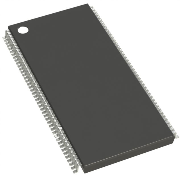
IS42S32200C1-7TLI
| Part Description |
IC DRAM 64MBIT PAR 86TSOP II |
|---|---|
| Quantity | 217 Available (as of June 9, 2026) |
| Product Category | Memory |
|---|---|
| Manufacturer | Integrated Silicon Solution Inc |
| Manufacturing Status | Obsolete |
| Manufacturer Standard Lead Time | Contact Us |
| Datasheet |
Specifications & Environmental
| Device Package | 86-TSOP II | Memory Format | DRAM | Technology | SDRAM | ||
|---|---|---|---|---|---|---|---|
| Memory Size | 64 Mbit | Access Time | 5.5 ns | Grade | Industrial | ||
| Clock Frequency | 143 MHz | Voltage | 3.15V ~ 3.45V | Memory Type | Volatile | ||
| Operating Temperature | -40°C ~ 85°C (TA) | Write Cycle Time Word Page | N/A | Packaging | 86-TFSOP (0.400", 10.16mm Width) | ||
| Mounting Method | Volatile | Memory Interface | Parallel | Memory Organization | 2M x 32 | ||
| Moisture Sensitivity Level | 3 (168 Hours) | RoHS Compliance | ROHS Compliant | REACH Compliance | REACH Unaffected | ||
| Qualification | N/A | ECCN | EAR99 | HTS Code | 8542.32.0002 |
Overview of IS42S32200C1-7TLI – IC DRAM 64MBIT PAR 86TSOP II
The IS42S32200C1-7TLI is a 64‑Mbit synchronous DRAM (SDRAM) organized as 524,288 × 32 × 4 banks (64 Mbit total) and designed for single 3.3 V memory systems. It implements a fully synchronous, pipelined architecture with internal bank interleaving to improve effective throughput.
With programmable burst lengths and CAS latency, LVTTL I/O, and options for industrial temperature operation, this device targets systems that require compact, high‑speed parallel DRAM memory with flexible timing and refresh management.
Key Features
- Core Architecture Fully synchronous SDRAM with all signals referenced to the positive clock edge; internal quad‑bank organization supports bank interleaving and pipeline operation.
- Memory Organization & Capacity 64 Mbit total capacity implemented as 524,288 × 32 × 4 banks (reported as 2M × 32 in the product specification).
- Performance & Timing Clock frequency rating includes a 143 MHz option; programmable CAS latency (2 or 3 clocks) and an access time of 5.5 ns (listed for relevant timing grade). Supports random column address every clock cycle and burst read/write modes.
- Burst and Sequencing Programmable burst lengths (1, 2, 4, 8, full page) and selectable burst sequence (sequential or interleave) for flexible data transfer patterns.
- Refresh & Power Modes Supports AUTO REFRESH and self‑refresh modes with 4096 refresh cycles every 64 ms, plus power‑down functionality for reduced standby power.
- Interface & Voltage LVTTL compatible I/O with a parallel memory interface. Single‑supply operation in the 3.15 V to 3.45 V range (nominal 3.3 V).
- Package & Mounting Available in 86‑pin TSOP II (400‑mil, 10.16 mm width) package; supplier device package listed as 86‑TSOP II.
- Temperature & Options Operating ambient range of −40 °C to 85 °C; device is available in industrial temperature grade and available in lead‑free option.
Typical Applications
- 3.3 V Memory Subsystems Use as system DRAM in 3.3 V memory architectures that require 64 Mbit density and synchronous burst access.
- High‑Speed Buffering and Burst Data Suitable for buffering and burst‑oriented data transfers where programmable burst length, burst sequence and CAS latency tuning are needed.
- Industrial Equipment Applicable in equipment requiring operation across −40 °C to 85 °C, leveraging the device’s industrial temperature grade option.
- Parallel SDRAM Implementations Integration into designs that require a LVTTL parallel SDRAM interface with quad‑bank organization for improved throughput.
Unique Advantages
- Quad‑Bank Architecture: Internal bank structure hides row access/precharge times and enables interleaved access for improved effective performance.
- Programmable Latency and Burst Control: CAS latency selectable between 2 and 3 clocks and multiple burst length/sequence options let designers tune timing for specific system requirements.
- Self‑Refresh and Power Management: Built‑in self‑refresh and power‑down modes with standard refresh timing (4096 cycles/64 ms) support low‑power standby and robust refresh management.
- Industrial Temperature Availability: Rated for −40 °C to 85 °C operation and offered in industrial grade, supporting applications with extended ambient requirements.
- Standard TSOP II Package: 86‑pin, 400‑mil TSOP II package (10.16 mm width) provides a common form factor for compact PCB implementations.
- Single‑Supply LVTTL Integration: Operates from a single 3.3 V supply with LVTTL I/O, simplifying integration into existing 3.3 V system designs.
Why Choose IS42S32200C1-7TLI?
The IS42S32200C1-7TLI delivers a compact 64 Mbit synchronous DRAM solution with flexible timing control, internal bank interleaving and industry‑grade temperature options. Its combination of programmable burst behavior, selectable CAS latency and self‑refresh capabilities makes it suitable for systems that need tunable high‑speed parallel memory and reliable refresh management.
This device is well suited to designs that require a 3.3 V LVTTL parallel SDRAM with an 86‑pin TSOP II footprint and industrial temperature operation. The availability of lead‑free and industrial variants supports longer lifecycle use and environmental options for constrained form‑factor memory subsystems.
Request a quote or submit a product inquiry to receive pricing, availability and lead‑time information for IS42S32200C1-7TLI.