IS42S32400E-6BLI
| Part Description |
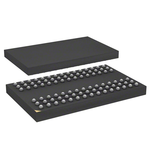
IC DRAM 128MBIT PAR 90TFBGA |
|---|---|
| Quantity | 377 Available (as of June 14, 2026) |

| Product Category | Memory |
|---|---|
| Manufacturer | Integrated Silicon Solution Inc |
| Manufacturing Status | Obsolete |
| Manufacturer Standard Lead Time | Contact Us |
| Datasheet |
Specifications & Environmental
| Device Package | 90-TFBGA (8x13) | Memory Format | DRAM | Technology | SDRAM | ||
|---|---|---|---|---|---|---|---|
| Memory Size | 128 Mbit | Access Time | 5.4 ns | Grade | Industrial | ||
| Clock Frequency | 166 MHz | Voltage | 3V ~ 3.6V | Memory Type | Volatile | ||
| Operating Temperature | -40°C ~ 85°C (TA) | Write Cycle Time Word Page | N/A | Packaging | 90-TFBGA | ||
| Mounting Method | Volatile | Memory Interface | Parallel | Memory Organization | 4M x 32 | ||
| Moisture Sensitivity Level | 3 (168 Hours) | RoHS Compliance | ROHS3 Compliant | REACH Compliance | REACH Unaffected | ||
| Qualification | N/A | ECCN | EAR99 | HTS Code | 8542.32.0002 |
Overview of IS42S32400E-6BLI – IC DRAM 128MBIT PAR 90TFBGA
The IS42S32400E-6BLI is a 128Mbit synchronous DRAM organized as 4M × 32 with a quad-bank architecture. It implements a fully synchronous pipeline architecture with all signals referenced to the rising edge of the clock.
Designed for systems requiring high-speed synchronous DRAM, this device delivers up to 166 MHz operation (‑6 timing), programmable burst modes and CAS latency options, and is supplied in a compact 90‑TFBGA package for board‑level integration.
Key Features
- Core Architecture Fully synchronous SDRAM organized as 1M × 32 × 4 banks for pipelined, high-speed data transfer.
- Memory Density & Organization 128 Mbit total capacity organized as 4M × 32.
- Performance Clock frequency up to 166 MHz (‑6 device); access time from clock as low as 5.4 ns at CAS latency = 3 for the ‑6 option.
- Programmable Burst and CAS Programmable burst lengths (1, 2, 4, 8, full page) and burst sequence (sequential/interleave); CAS latency selectable (2 or 3 clocks).
- Refresh and Power Management Supports Auto Refresh (CBR) and Self Refresh. Refresh cycles vary by grade: 4096 refresh cycles every 16 ms (A2 grade) or 64 ms (Commercial/Industrial/A1 grade).
- Interface Parallel SDRAM interface with LVTTL-compatible signals; random column address every clock cycle.
- Power Single power supply operation at 3.3 V (specified 3.0 V to 3.6 V range).
- Package & Temperature 90‑ball TF‑BGA (8 × 13) package; specified operating temperature range −40 °C to +85 °C (TA).
- Operational Commands Supports burst read/write, burst read/single write, burst termination by burst stop and precharge commands, and internal bank architecture for row access/precharge hiding.
Typical Applications
- Synchronous memory subsystems Implementation as high-speed SDRAM in systems that require a parallel synchronous DRAM interface and programmable burst behavior.
- Embedded digital systems Use where a 128 Mbit volatile SDRAM with selectable CAS latency and self/auto refresh is required for temporary data storage.
- Board-level memory integration Integration into designs that need a compact 90‑TFBGA DRAM package operating from a 3.3 V supply and supporting industrial temperature ranges.
Unique Advantages
- Selectable high-speed timing: 166 MHz clock option with low access time (5.4 ns at CL=3) enables support for faster synchronous data paths.
- Flexible burst control: Programmable burst lengths and sequence options simplify system memory access patterns and burst optimization.
- Power supply compatibility: Single 3.3 V supply (3.0–3.6 V range) matches common 3.3 V memory systems for straightforward integration.
- Compact package footprint: 90‑TFBGA (8×13) package reduces PCB area for dense board designs.
- Robust refresh options: Auto Refresh and Self Refresh with defined refresh cycle modes across device grades provide predictable data retention behavior.
- Programmable timing trade-offs: CAS latency selectable between 2 and 3 clocks to balance frequency and access time requirements.
Why Choose IS42S32400E-6BLI?
The IS42S32400E-6BLI positions itself as a practical 128 Mbit synchronous DRAM option for designs that require a compact, parallel SDRAM device with programmable burst and timing features. Its 4M × 32 organization and internal quad-bank architecture support pipelined, high-speed transfers while the 3.3 V single-supply operation aligns with common memory subsystems.
This device is suitable for engineers specifying board-level SDRAM where selectable CAS latency, managed refresh modes, and a small TF‑BGA footprint are important. The combination of documented timing (including 166 MHz operation and 5.4 ns access time at CL=3 for the ‑6 option) and supported refresh/self-refresh functionality offers predictable behavior for evaluation and integration into synchronous memory designs.
Request a quote or submit an inquiry to start procurement or evaluation of the IS42S32400E-6BLI for your design.