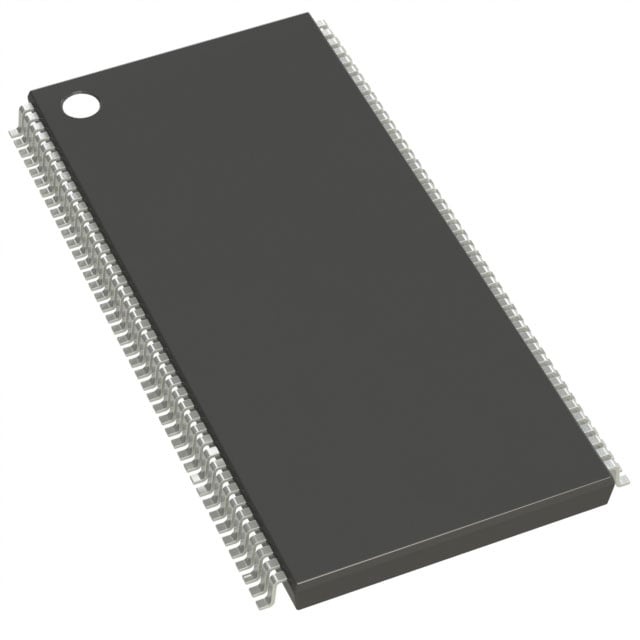
IS42S32400E-6TL
| Part Description |
IC DRAM 128MBIT PAR 86TSOP II |
|---|---|
| Quantity | 76 Available (as of June 15, 2026) |

| Product Category | Memory |
|---|---|
| Manufacturer | Integrated Silicon Solution Inc |
| Manufacturing Status | Obsolete |
| Manufacturer Standard Lead Time | Contact Us |
| Datasheet |
Specifications & Environmental
| Device Package | 86-TSOP II | Memory Format | DRAM | Technology | SDRAM | ||
|---|---|---|---|---|---|---|---|
| Memory Size | 128 Mbit | Access Time | 5.4 ns | Grade | Commercial | ||
| Clock Frequency | 166 MHz | Voltage | 3V ~ 3.6V | Memory Type | Volatile | ||
| Operating Temperature | 0°C ~ 70°C (TA) | Write Cycle Time Word Page | N/A | Packaging | 86-TFSOP (0.400", 10.16mm Width) | ||
| Mounting Method | Volatile | Memory Interface | Parallel | Memory Organization | 4M x 32 | ||
| Moisture Sensitivity Level | 3 (168 Hours) | RoHS Compliance | ROHS3 Compliant | REACH Compliance | REACH Unaffected | ||
| Qualification | N/A | ECCN | EAR99 | HTS Code | 8542.32.0002 |
Overview of IS42S32400E-6TL – IC DRAM 128MBIT PAR 86TSOP II
The IS42S32400E-6TL is a 128 Mbit synchronous DRAM organized as 4M × 32 with a quad-bank architecture. It implements a pipelined, fully synchronous design with all signals referenced to the positive clock edge for high-speed parallel memory operations.
This device is intended for systems requiring a compact, parallel SDRAM solution with programmable burst and latency options, operating from a single 3.3 V supply in an 86‑pin TSOP II package and a commercial temperature range of 0 °C to 70 °C.
Key Features
- Core / Architecture Quad-bank, pipelined SDRAM architecture arranged as 1M × 32 × 4 banks to support interleaved and hidden row operations for improved throughput.
- Memory Capacity & Organization 128 Mbit total capacity organized as 4M × 32, suitable for parallel memory subsystems requiring 32‑bit data width.
- Clock & Performance Support for up to 166 MHz clock frequency (‑6 device) with an access time from clock of 5.4 ns at CAS latency = 3.
- Programmable Burst & Latency Programmable burst lengths (1, 2, 4, 8, full page) and selectable burst sequence (sequential/interleave); CAS latency programmable to 2 or 3 clocks.
- Refresh & Retention Auto Refresh (CBR) and Self Refresh supported; 4096 refresh cycles per refresh interval according to device grade options.
- Interface & Signaling Parallel memory interface with LVTTL-compatible signals for synchronous control referenced to the rising clock edge.
- Power Single power supply operation at 3.3 V (3.0 V to 3.6 V specified range), simplifying system power rails.
- Package & Temperature 86‑pin TSOP II (10.16 mm width) package; commercial operating temperature range of 0 °C to 70 °C (TA).
Typical Applications
- System memory — Provides 128 Mbit of synchronous parallel DRAM for designs that require a 4M × 32 memory organization and quad‑bank operation.
- Buffering and frame storage — Pipelined, clocked operation and programmable burst modes support high-speed temporary data buffering and throughput-oriented tasks.
- Memory controller validation — Standard SDRAM feature set (LVTTL interface, programmable CAS, auto/self refresh) makes it suitable for testing and validating parallel SDRAM controllers.
- Refresh‑sensitive designs — Auto and self refresh capabilities with configurable refresh cycles support systems that require managed refresh behavior.
Unique Advantages
- High-frequency operation: Supports 166 MHz clocking on the ‑6 device with a 5.4 ns access time (CAS‑3), enabling fast synchronous transfers.
- Flexible timing control: Programmable CAS latency (2/3) and multiple burst length/sequence options allow tuning for controller and system timing requirements.
- Quad-bank pipelining: Internal bank architecture hides row access/precharge latencies to maintain throughput in interleaved access patterns.
- Single-supply integration: Operates from a single 3.3 V supply (3.0–3.6 V range), simplifying power rail design.
- Compact, industry-standard package: 86‑pin TSOP II (10.16 mm width) provides a space-efficient footprint for board-level memory implementations.
- Refresh management: Supports Auto Refresh and Self Refresh with defined refresh cycle counts to ensure data retention across operating conditions.
Why Choose IS42S32400E-6TL?
The IS42S32400E-6TL delivers a compact 128 Mbit synchronous DRAM solution with programmable timing, burst control and a quad‑bank pipelined architecture to support high-speed parallel memory designs. Its 166 MHz capability (for the ‑6 variant), LVTTL interface and single 3.3 V supply make it suitable for systems that need a standardized SDRAM building block with adjustable performance characteristics.
This device is well suited to designers seeking a reliable, easily integrated parallel SDRAM component in an 86‑TSOP II package, offering configurable refresh and latency options to align with system memory controllers and timing budgets.
Request a quote or submit a parts inquiry to receive pricing and availability information for IS42S32400E-6TL.