IS42S32400E-7BL
| Part Description |
IC DRAM 128MBIT PAR 90TFBGA |
|---|---|
| Quantity | 998 Available (as of June 15, 2026) |

| Product Category | Memory |
|---|---|
| Manufacturer | Integrated Silicon Solution Inc |
| Manufacturing Status | Obsolete |
| Manufacturer Standard Lead Time | Contact Us |
| Datasheet |
Specifications & Environmental
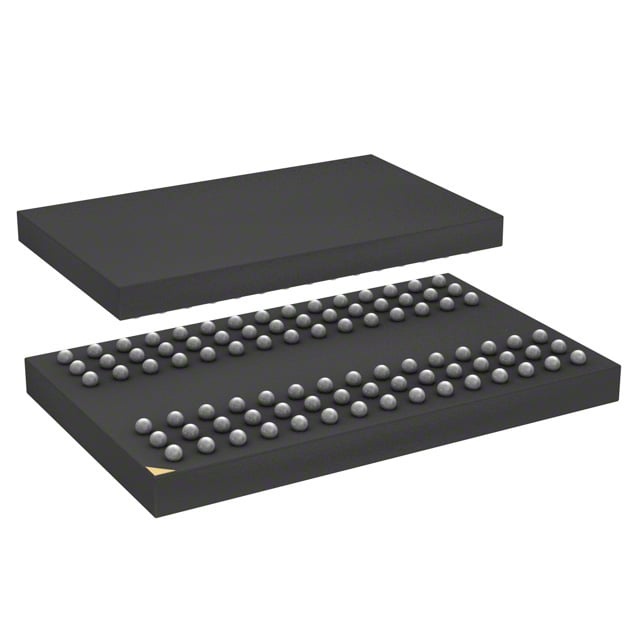
| Device Package | 90-TFBGA (8x13) | Memory Format | DRAM | Technology | SDRAM | ||
|---|---|---|---|---|---|---|---|
| Memory Size | 128 Mbit | Access Time | 5.4 ns | Grade | Commercial | ||
| Clock Frequency | 143 MHz | Voltage | 3V ~ 3.6V | Memory Type | Volatile | ||
| Operating Temperature | 0°C ~ 70°C (TA) | Write Cycle Time Word Page | N/A | Packaging | 90-TFBGA | ||
| Mounting Method | Volatile | Memory Interface | Parallel | Memory Organization | 4M x 32 | ||
| Moisture Sensitivity Level | 3 (168 Hours) | RoHS Compliance | ROHS Compliant | REACH Compliance | REACH Unaffected | ||
| Qualification | N/A | ECCN | EAR99 | HTS Code | 8542.32.0002 |
Overview of IS42S32400E-7BL – 128 Mbit SDRAM, 4M × 32, 90‑TFBGA
The IS42S32400E-7BL is a 128 Mbit synchronous DRAM organized as 4M × 32 with four internal banks and pipeline architecture. It operates as a parallel SDRAM with signals referenced to the rising edge of the clock and supports a single 3.3 V power supply range.
Designed for systems that require compact, high‑speed parallel memory, this device delivers programmable burst operation, selectable CAS latency, and refresh modes suitable for commercial temperature designs (0 °C to +70 °C).
Key Features
- Core / Memory Organization 128 Mbit SDRAM configured as 1M × 32 × 4 banks (4M × 32 overall) for 32‑bit data paths and internal bank management.
- Synchronous, Pipeline Architecture Fully synchronous operation with all inputs and outputs referenced to the positive clock edge for predictable timing and pipelined data transfer.
- Performance / Timing Clock frequency options include 166, 143 and 133 MHz; the –7 speed grade provides 143 MHz operation and CAS latency options of 2 or 3. Access time from clock for CAS‑3 is 5.4 ns.
- Burst & Latency Control Programmable burst lengths (1, 2, 4, 8, full page) and programmable burst sequence (sequential/interleave) with burst termination via burst stop or precharge commands.
- Refresh and Low‑Power Modes Supports auto refresh (CBR) and self‑refresh; 4096 refresh cycles with timing options (16 ms for A2 grade or 64 ms for commercial/other grades as defined in the datasheet).
- Interface & Logic Levels LVTTL interface and parallel memory interface for direct connection to 3.3 V logic systems.
- Power Supply Single power supply operation at 3.3 V (specified in data as 3.3 V ±0.3 V; device data lists allowable 3.0 V to 3.6 V).
- Package & Mounting 90‑ball TF‑BGA (8 × 13) package for compact board footprint and surface‑mount assembly; commercial operating temperature range of 0 °C to +70 °C.
Typical Applications
- Embedded systems memory Provides 128 Mbit of parallel SDRAM for embedded platforms requiring a 32‑bit data interface and synchronous timing.
- Data buffering Programmable burst lengths and burst sequencing make the device suitable for high‑throughput buffering and temporary storage in digital subsystems.
- System controllers and peripherals LVTTL interface and 3.3 V single‑supply operation simplify integration with 3.3 V controller cores and peripheral logic.
Unique Advantages
- Configurable performance Selectable CAS latency (2 or 3) and multiple clock frequency grades let designers balance latency and throughput for target use cases.
- Flexible burst operation Programmable burst lengths and sequence modes enable efficient block transfers and optimized memory access patterns.
- Single 3.3 V supply Standard 3.3 V operation (3.0 V–3.6 V range) reduces power‑domain complexity in 3.3 V systems.
- Compact BGA package 90‑ball TF‑BGA (8×13) minimizes PCB area while supporting surface‑mount assembly processes.
- Predictable synchronous timing Fully synchronous design and pipeline architecture provide deterministic timing referenced to the clock rising edge.
- Refresh and power management Auto and self‑refresh options with documented refresh intervals offer control over data retention and power behavior.
Why Choose IS42S32400E-7BL?
The IS42S32400E-7BL delivers 128 Mbit of parallel synchronous DRAM in a compact 90‑TFBGA package with programmable latency and burst features for flexible system integration. Its single 3.3 V supply, LVTTL interface, and pipeline architecture make it suitable for designs that need deterministic, high‑speed memory with standard commercial temperature operation.
This device is well suited to engineers building systems that require a 32‑bit SDRAM interface, configurable performance (clock and CAS latency), and compact board‑level implementation. The documented refresh, timing and interface options support predictable behavior across the stated commercial operating range.
Request a quote or submit a specification request to obtain pricing and availability for the IS42S32400E-7BL. Our team can provide further technical details and support for integration into your design.