IS42S32400E-7BLI-TR
| Part Description |
IC DRAM 128MBIT PAR 90TFBGA |
|---|---|
| Quantity | 844 Available (as of June 10, 2026) |
| Product Category | Memory |
|---|---|
| Manufacturer | Integrated Silicon Solution Inc |
| Manufacturing Status | Obsolete |
| Manufacturer Standard Lead Time | Contact Us |
| Datasheet |
Specifications & Environmental
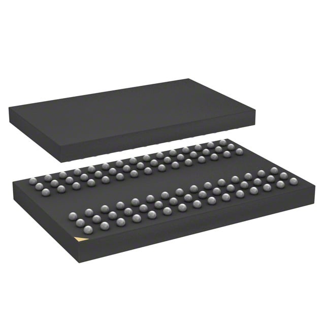
| Device Package | 90-TFBGA (8x13) | Memory Format | DRAM | Technology | SDRAM | ||
|---|---|---|---|---|---|---|---|
| Memory Size | 128 Mbit | Access Time | 5.4 ns | Grade | Industrial | ||
| Clock Frequency | 143 MHz | Voltage | 3V ~ 3.6V | Memory Type | Volatile | ||
| Operating Temperature | -40°C ~ 85°C (TA) | Write Cycle Time Word Page | N/A | Packaging | 90-TFBGA | ||
| Mounting Method | Volatile | Memory Interface | Parallel | Memory Organization | 4M x 32 | ||
| Moisture Sensitivity Level | 3 (168 Hours) | RoHS Compliance | ROHS3 Compliant | REACH Compliance | REACH Unaffected | ||
| Qualification | N/A | ECCN | EAR99 | HTS Code | 8542.32.0002 |
Overview of IS42S32400E-7BLI-TR – IC DRAM 128MBIT PAR 90TFBGA
The IS42S32400E-7BLI-TR is a 128 Mbit synchronous DRAM organized as 4M × 32 with a quad-bank architecture. It is a pipeline, fully synchronous SDRAM device designed for 3.3 V memory systems with a parallel LVTTL interface.
This device targets applications that require high-speed, predictable memory access with programmable burst operation and internal bank management to optimize row access and precharge behavior. Its package and temperature rating support deployment in designs requiring industrial temperature operation.
Key Features
- Core / Memory Organization The device is organized as 4M × 32 (1M × 32 × 4 banks) providing 128 Mbit of SDRAM capacity.
- Performance Clock frequency up to 143 MHz (–7 device), with an access time from clock of 5.4 ns at CAS latency = 3.
- Burst and Latency Control Programmable burst lengths (1, 2, 4, 8, full page) and burst sequence (sequential/interleave); programmable CAS latency (2 or 3 clocks).
- Banking and Refresh Quad-bank internal architecture for hiding row access/precharge; supports Auto Refresh (CBR) and Self Refresh with 4096 refresh cycles per refresh interval as specified by grade.
- Interface Parallel LVTTL interface suitable for synchronous memory systems; random column address every clock cycle.
- Power Single power supply: 3.0 V to 3.6 V (3.3 V ±0.3 V operation documented in datasheet).
- Package & Mounting 90-ball TF-BGA package (90-TFBGA, 8 × 13) for compact board-level mounting.
- Operating Temperature Rated for –40°C to +85°C (TA) for the industrial-grade variant.
Typical Applications
- 3.3 V memory systems Acts as synchronous DRAM in 3.3 V memory subsystems requiring a parallel LVTTL SDRAM interface.
- High-speed buffering Useful for designs requiring burst read/write buffering and predictable CAS-latency performance.
- Industrial electronics Industrial temperature range (–40°C to +85°C) makes the device suitable for temperature‑sensitive embedded systems.
Unique Advantages
- Deterministic synchronous operation Fully synchronous design with all signals referenced to the rising clock edge enables predictable timing and integration into synchronous memory controllers.
- Flexible burst control Programmable burst length and sequence options allow tuning for throughput or random access efficiency based on application needs.
- Quad-bank architecture Internal banking hides row access and precharge latency, improving effective throughput for interleaved access patterns.
- Industrial temperature rating Rated operation from –40°C to +85°C supports deployment in harsher environmental conditions.
- Compact BGA package 90-TFBGA (8 × 13) provides a small board footprint for space-constrained designs.
- Standard 3.3 V supply Operates from 3.0 V to 3.6 V (3.3 V ±0.3 V documented), matching common memory system voltages.
Why Choose IS42S32400E-7BLI-TR?
The IS42S32400E-7BLI-TR provides a straightforward, specification-driven synchronous DRAM solution for designs that require 128 Mbit of parallel SDRAM with programmable burst control, selectable CAS latency, and an internal quad-bank architecture to improve data throughput. Its LVTTL interface and standard 3.3 V supply make it compatible with typical synchronous memory subsystems.
This part is well suited to engineers and procurement teams building industrial-temperature embedded systems or other applications that need predictable synchronous memory behavior in a compact 90-TFBGA package. The combination of timing options, refresh modes, and standard supply voltage simplifies integration and long-term system planning.
Request a quote or submit an inquiry for pricing and availability of the IS42S32400E-7BLI-TR to receive detailed lead-time and ordering information.