IS42S32400E-6BLI-TR
| Part Description |
IC DRAM 128MBIT PAR 90TFBGA |
|---|---|
| Quantity | 1,420 Available (as of June 15, 2026) |

| Product Category | Memory |
|---|---|
| Manufacturer | Integrated Silicon Solution Inc |
| Manufacturing Status | Obsolete |
| Manufacturer Standard Lead Time | Contact Us |
| Datasheet |
Specifications & Environmental
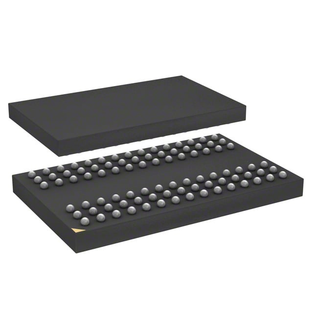
| Device Package | 90-TFBGA (8x13) | Memory Format | DRAM | Technology | SDRAM | ||
|---|---|---|---|---|---|---|---|
| Memory Size | 128 Mbit | Access Time | 5.4 ns | Grade | Industrial | ||
| Clock Frequency | 166 MHz | Voltage | 3V ~ 3.6V | Memory Type | Volatile | ||
| Operating Temperature | -40°C ~ 85°C (TA) | Write Cycle Time Word Page | N/A | Packaging | 90-TFBGA | ||
| Mounting Method | Volatile | Memory Interface | Parallel | Memory Organization | 4M x 32 | ||
| Moisture Sensitivity Level | 3 (168 Hours) | RoHS Compliance | ROHS3 Compliant | REACH Compliance | REACH Unaffected | ||
| Qualification | N/A | ECCN | EAR99 | HTS Code | 8542.32.0002 |
Overview of IS42S32400E-6BLI-TR – IC DRAM 128MBIT PAR 90TFBGA
The IS42S32400E-6BLI-TR is a 128 Mbit synchronous DRAM organized as 4M × 32 with a quad-bank architecture and pipeline access. It implements fully synchronous operation with signals referenced to the rising edge of the clock and is designed for systems requiring high-speed SDRAM memory.
Key capabilities include operation at a 166 MHz clock (CAS latency = 3), a 3.3 V supply range, programmable burst modes and refresh options—making it suitable for designs that need predictable, high-throughput parallel DRAM behavior in a compact 90-TFBGA package.
Key Features
- Memory Core The device is organized as 4M × 32 (128 Mbit) with internal quad-bank architecture to hide row access and precharge latency.
- Synchronous SDRAM Fully synchronous operation with all signals referenced to the rising clock edge; clock frequency support includes 166 MHz, 143 MHz and 133 MHz options.
- Timing and Performance CAS latency programmable to 2 or 3 clocks; for the -6 grade CAS latency = 3 yields a 166 MHz clock and an access time from clock of 5.4 ns.
- Burst and Access Modes Programmable burst length (1, 2, 4, 8, full page) and burst sequence (sequential/interleave); supports burst read/write and burst read/single write with burst termination commands.
- Refresh and Self-Refresh Auto refresh and self-refresh supported; refresh count is 4096 cycles with timing options of 16 ms (A2 grade) or 64 ms (Commercial/Industrial/A1 grade) as specified by device grade.
- Interface and Logic Levels LVTTL interface signaling; random column address capability every clock cycle.
- Power Single power supply: 3.3 V ± 0.3 V (specified supply range 3.0 V to 3.6 V).
- Package Supplied in a 90-ball TF-BGA (90-TFBGA, 8×13) package suitable for board-level integration.
- Operating Temperature Rated for −40°C to +85°C (TA) for industrial-grade operation as provided for this product variant.
Typical Applications
- System Memory Expansion Used as parallel SDRAM for systems that require synchronous, banked DRAM storage with programmable burst and latency behavior.
- High-Speed Buffering Serves as a high-throughput buffer where 166 MHz clock operation and burst transfers improve sustained data movement.
- Embedded and Industrial Electronics Suitable for embedded designs requiring industrial temperature operation (−40°C to +85°C) and standard 3.3 V supply.
Unique Advantages
- High-frequency capability: 166 MHz operation (CAS = 3) supports low-latency access with a 5.4 ns access time from clock for the -6 device grade.
- Flexible burst control: Programmable burst lengths and sequence modes enable efficient data transfer patterns tailored to application needs.
- Quad-bank architecture: Internal bank structure helps hide row access/precharge latency and supports sustained throughput.
- Standard supply and interface: Operates from a 3.3 V supply with LVTTL signaling for straightforward system integration.
- Compact BGA package: 90-TFBGA (8×13) package reduces board footprint while providing a high-pin-count DRAM solution.
- Industrial temperature rating: −40°C to +85°C operation supports deployment in temperature-sensitive environments.
Why Choose IS42S32400E-6BLI-TR?
The IS42S32400E-6BLI-TR combines a 4M × 32 organization and quad-bank synchronous DRAM architecture with programmable burst and refresh features to deliver predictable, high-throughput parallel memory behavior. Its 166 MHz capable timing (CAS = 3) and 5.4 ns access timing (from clock) make it suitable for designs that demand low-latency SDRAM performance.
This device is appropriate for engineers specifying compact, board-level DRAM in industrial-temperature systems powered from a standard 3.3 V supply. The feature set—programmable CAS, burst modes, auto/self-refresh and LVTTL interface—offers configurability for a range of system memory and buffering needs.
Request a quote or contact sales to discuss availability, lead times and volume pricing for the IS42S32400E-6BLI-TR.