IS42S83200B-7TLI
| Part Description |
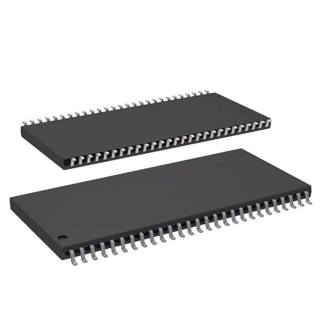
IC DRAM 256MBIT PAR 54TSOP II |
|---|---|
| Quantity | 658 Available (as of June 17, 2026) |

| Product Category | DRAM Memory |
|---|---|
| Manufacturer | Integrated Silicon Solution Inc |
| Manufacturing Status | Obsolete |
| Manufacturer Standard Lead Time | Contact Us |
| Datasheet |
Specifications & Environmental
| Device Package | 54-TSOP II | Memory Format | DRAM | Technology | SDRAM | ||
|---|---|---|---|---|---|---|---|
| Memory Size | 256 Mbit | Access Time | 5.4 ns | Grade | Industrial | ||
| Clock Frequency | 143 MHz | Voltage | 3V ~ 3.6V | Memory Type | Volatile | ||
| Operating Temperature | -40°C ~ 85°C (TA) | Write Cycle Time Word Page | N/A | Packaging | 54-TSOP (0.400", 10.16mm Width) | ||
| Mounting Method | Volatile | Memory Interface | Parallel | Memory Organization | 32M x 8 | ||
| Moisture Sensitivity Level | 3 (168 Hours) | RoHS Compliance | ROHS3 Compliant | REACH Compliance | REACH Unaffected | ||
| Qualification | N/A | ECCN | EAR99 | HTS Code | 8542.32.0024 |
Overview of IS42S83200B-7TLI – IC DRAM 256MBIT PAR 54TSOP II
The IS42S83200B-7TLI is a 256 Mbit synchronous DRAM organized as 32M × 8 with a parallel LVTTL interface. It is a fully synchronous, quad-bank SDRAM designed for high-speed burst transfers with internal bank interleaving and pipeline architecture.
This device is optimized for designs requiring programmable burst lengths and CAS latencies, and it is available in a 54-pin TSOP-II package with an industrial operating temperature range for use in temperature-challenging environments.
Key Features
- Memory Core 256 Mbit SDRAM organized as 32M × 8 with four internal banks to support interleaved access and row precharge hiding.
- Performance Supports clock frequencies of 166, 143 and 133 MHz (the -7 speed grade corresponds to 143 MHz). Access time from clock is 5.4 ns at CAS latency = 3.
- Burst and Latency Programmable burst lengths (1, 2, 4, 8, full page) and selectable burst sequences (sequential/interleave). Programmable CAS latency options of 2 and 3 clocks.
- Interface & Operation Fully synchronous operation with all signals referenced to the rising edge of CLK; LVTTL-compatible inputs and random column address capability every clock cycle.
- Power Designed for 3.0 V to 3.6 V operation (datasheet indicates VDD = 3.3 V / VDDQ = 3.3 V for the IS42S83200B family).
- Refresh & Power Management Auto Refresh (CBR), Self Refresh and 8K refresh cycles every 64 ms; includes power-down mode and auto precharge support.
- Package & Temperature Supplied in a 54-pin TSOP-II (0.400", 10.16 mm width) package and specified for an operating temperature range of −40 °C to 85 °C (TA).
- Options Available in industrial temperature grades and offered in lead-free versions according to the device family notes.
Typical Applications
- High-speed buffering and caching Burst read/write capability and programmable burst lengths enable high-throughput temporary storage and data buffering in synchronous systems.
- System memory for parallel interfaces Fully synchronous LVTTL interface and random column access each clock cycle facilitate integration into parallel memory subsystems.
- Industrial equipment Industrial temperature rating (−40 °C to 85 °C) allows use in temperature-challenging control and instrumentation platforms.
- Space-constrained PCB designs 54-pin TSOP-II packaging provides a compact footprint for designs requiring board-level SDRAM density.
Unique Advantages
- Flexible burst control: Programmable burst lengths and sequence options let designers tune transfer patterns for application-specific throughput and latency.
- Bank interleave architecture: Four internal banks and internal precharge mechanisms help hide row access times and improve sustained data throughput.
- Multiple speed grades: Available clock frequency grades (166, 143, 133 MHz) and CAS latency options provide performance scalability for different design targets.
- Industrial temperature availability: Specified operation from −40 °C to 85 °C supports deployment in harsh or wide-temperature environments.
- Compact package: 54-pin TSOP-II (0.400", 10.16 mm) offers a small-footprint solution for board-level memory expansion.
- Power management features: Auto Refresh, Self Refresh and power-down modes reduce system-level power during idle periods.
Why Choose IS42S83200B-7TLI?
The IS42S83200B-7TLI combines synchronous, pipelined SDRAM architecture with programmable burst and latency options to deliver predictable, high-speed memory performance for parallel interface systems. Its quad-bank internal organization and automatic precharge modes enable efficient, continuous data transfers while minimizing access penalties.
With support for industry-standard 3.0–3.6 V supplies (datasheet nominal VDD = 3.3 V), LVTTL signaling, industrial temperature rating, and a compact 54-pin TSOP-II package, this device is well-suited for designs that require reliable, scalable volatile memory in constrained footprints and temperature-challenging environments.
Request a quote or submit a sales inquiry to obtain pricing, availability and additional product options for the IS42S83200B-7TLI.