IS42S83200D-6TL
| Part Description |
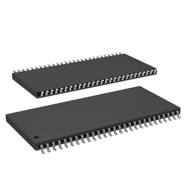
IC DRAM 256MBIT PAR 54TSOP II |
|---|---|
| Quantity | 254 Available (as of June 18, 2026) |

| Product Category | DRAM Memory |
|---|---|
| Manufacturer | Integrated Silicon Solution Inc |
| Manufacturing Status | Obsolete |
| Manufacturer Standard Lead Time | Contact Us |
| Datasheet |
Specifications & Environmental
| Device Package | 54-TSOP II | Memory Format | DRAM | Technology | SDRAM | ||
|---|---|---|---|---|---|---|---|
| Memory Size | 256 Mbit | Access Time | 5.4 ns | Grade | Commercial | ||
| Clock Frequency | 166 MHz | Voltage | 3V ~ 3.6V | Memory Type | Volatile | ||
| Operating Temperature | 0°C ~ 70°C (TA) | Write Cycle Time Word Page | N/A | Packaging | 54-TSOP (0.400", 10.16mm Width) | ||
| Mounting Method | Volatile | Memory Interface | Parallel | Memory Organization | 32M x 8 | ||
| Moisture Sensitivity Level | 3 (168 Hours) | RoHS Compliance | ROHS Compliant | REACH Compliance | REACH Unaffected | ||
| Qualification | N/A | ECCN | EAR99 | HTS Code | 8542.32.0024 |
Overview of IS42S83200D-6TL – IC DRAM 256MBIT PAR 54TSOP II
The IS42S83200D-6TL is a 256‑Mbit synchronous DRAM organized as 32M × 8 with four internal banks. It uses a pipelined, fully synchronous architecture with all signals referenced to the rising edge of the clock to enable high‑speed data transfer and burst operations.
This device is intended for applications requiring parallel SDRAM with programmable burst lengths and sequences, low access latency, and a standard 54‑pin TSOP‑II package footprint. Key value points include 166 MHz clock operation, programmable CAS latency, and support for auto and self refresh modes.
Key Features
- Memory Architecture 256‑Mbit SDRAM organized as 32M × 8 with 4 internal banks and pipeline architecture to support continuous data flow.
- Performance & Timing Supports clock frequency up to 166 MHz and access time of 5.4 ns (CAS latency = 3); programmable CAS latency options of 2 or 3 clocks.
- Burst Operations Programmable burst lengths (1, 2, 4, 8, full page) and selectable burst sequence (sequential/interleave) for flexible data transfer patterns.
- Refresh & Power Management Auto Refresh (CBR) and Self Refresh supported; refresh rate options include 8K cycles every 16 ms (A2) or 64 ms (commercial/A1) as specified.
- Interface Fully synchronous LVTTL interface with parallel memory access and random column address capability every clock cycle.
- Supply & Operating Range Single power supply: 3.3 V ±0.3 V (3.0 V–3.6 V). Commercial operating temperature range: 0°C to +70°C (TA).
- Package 54‑pin TSOP‑II package (0.400", 10.16 mm width) for compact board placement and standard mounting.
Typical Applications
- High‑speed buffering For systems that require synchronous, pipelined memory to support continuous data streams and burst transfers.
- Parallel system memory As parallel SDRAM for designs needing organized 32M × 8 memory with programmable CAS latency and burst control.
- Data transfer and caching Suitable where low access time (5.4 ns at CL=3) and programmable burst lengths improve throughput for read/write bursts.
Unique Advantages
- High clock capability: Operates at up to 166 MHz (CL=3), enabling faster synchronous transfers within supported timing.
- Flexible burst control: Programmable burst length and sequence allow optimization of transfer patterns for different workloads.
- Low access latency: 5.4 ns access time (CAS latency = 3) supports designs that need quick data availability.
- Built‑in refresh management: Auto and self refresh modes with specified 8K refresh cycles provide reliable data retention management.
- Standard packaging: 54‑pin TSOP‑II package provides a common footprint for compact board layouts.
- Single‑supply operation: 3.0–3.6 V operation (nominal 3.3 V) simplifies power rail requirements.
Why Choose IC DRAM 256MBIT PAR 54TSOP II?
The IS42S83200D‑6TL delivers a 256‑Mbit synchronous DRAM solution that combines a pipelined architecture, programmable burst modes, and low access time to support high‑speed parallel memory applications. Its 32M × 8 organization, LVTTL interface, and 54‑pin TSOP‑II package make it suitable for designs that require predictable, synchronous memory behavior and flexible burst control.
This device is appropriate for engineers specifying synchronous DRAM at up to 166 MHz who need on‑die bank management, refresh support, and standard packaging for integration into parallel memory subsystems.
Request a quote or submit an inquiry to receive pricing and availability information for the IS42S83200D-6TL.