IS43DR16160A-37CBLI-TR
| Part Description |
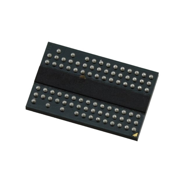
IC DRAM 256MBIT PAR 84TWBGA |
|---|---|
| Quantity | 710 Available (as of June 14, 2026) |

| Product Category | Memory |
|---|---|
| Manufacturer | Integrated Silicon Solution Inc |
| Manufacturing Status | Obsolete |
| Manufacturer Standard Lead Time | Contact Us |
| Datasheet |
Specifications & Environmental
| Device Package | 84-TWBGA (8x12.5) | Memory Format | DRAM | Technology | SDRAM - DDR2 | ||
|---|---|---|---|---|---|---|---|
| Memory Size | 256 Mbit | Access Time | 500 ps | Grade | Industrial | ||
| Clock Frequency | 266 MHz | Voltage | 1.7V ~ 1.9V | Memory Type | Volatile | ||
| Operating Temperature | -40°C ~ 85°C (TA) | Write Cycle Time Word Page | 15 ns | Packaging | 84-TFBGA | ||
| Mounting Method | Volatile | Memory Interface | Parallel | Memory Organization | 16M x 16 | ||
| Moisture Sensitivity Level | 3 (168 Hours) | RoHS Compliance | ROHS3 Compliant | REACH Compliance | REACH Unaffected | ||
| Qualification | N/A | ECCN | EAR99 | HTS Code | 8542.32.0024 |
Overview of IS43DR16160A-37CBLI-TR – 256Mbit DDR2 DRAM, 84-TWBGA
The IS43DR16160A-37CBLI-TR is a 256Mbit DDR2 SDRAM organized as 16M × 16 with a parallel memory interface. It implements a double-data-rate architecture with a 4-bit prefetch to deliver two data transfers per clock cycle and includes on-chip features to support high-speed synchronous operation.
Key device characteristics in the specification set include a 266 MHz clock frequency rating, supply voltage range of 1.7 V to 1.9 V, programmable CAS latencies, on-die termination, and an 84-ball thin wide BGA package (8 mm × 12.5 mm). The device is specified for an ambient operating temperature range of -40°C to 85°C.
Key Features
- Core / Memory Architecture 16M × 16 organization (256 Mbit) with 4 internal banks and a 4-bit prefetch architecture for DDR2 operation.
- Double-Data-Rate Interface Two data transfers per clock cycle plus differential data strobe (DQS / DQS̅) to support synchronous data capture.
- Timing and Programmability Programmable CAS latency (CL = 3, 4, 5, 6) and programmable additive latency (AL = 0–5); programmable burst lengths of 4 or 8 and posted CAS supported.
- Signal Conditioning On-chip DLL to align DQ and DQS transitions with CK, adjustable data-output drive strength, and on-die termination (ODT) for signal integrity.
- Performance Supported cycle times and speed grades include timing targets down to 2.5 ns at CL = 6; typical access time reported as 500 ps.
- Power VDD and VDDQ operating range 1.7 V to 1.9 V (JEDEC 1.8 V ±0.1 V compatibility documented in datasheet excerpts).
- Package & Temperature 84-TWBGA (8 mm × 12.5 mm) supplier package; ambient operating temperature range −40°C to 85°C (TA).
Typical Applications
- Parallel memory subsystems — Used where a 16M × 16 DDR2 memory interface is required for system memory or local DRAM buffering.
- High-speed synchronous designs — Applicable to designs that utilize double-data-rate transfers and require programmable CAS latency and burst control.
- Board-level DRAM integration — Suitable for PCB implementations needing an 84-ball WBGA package footprint (8 mm × 12.5 mm) and standard DDR2 signaling.
Unique Advantages
- Flexible timing control: Programmable CAS and additive latency options (CL 3–6, AL 0–5) enable tuning for different system timing requirements.
- Signal integrity features: On-chip DLL, differential DQS, adjustable drive strength and on-die termination help simplify board signal timing and termination strategies.
- DDR2 double-data-rate throughput: 4-bit prefetch and two transfers per clock cycle provide higher effective bandwidth versus single-data-rate memory.
- Compact package: 84-TWBGA (8 mm × 12.5 mm) package supports dense board layouts while maintaining a parallel DDR2 interface.
- Wide operating conditions: Specified supply range of 1.7 V–1.9 V and ambient temperature rating from −40°C to 85°C for broad deployment scenarios.
Why Choose IS43DR16160A-37CBLI-TR?
The IS43DR16160A-37CBLI-TR delivers a standardized DDR2 SDRAM feature set—programmable latencies, burst control, ODT, DLL alignment and differential strobes—packaged in an 84-ball TWBGA footprint. These characteristics make it a practical choice for engineers implementing parallel DDR2 memory subsystems that require configurable timing, on-die signal conditioning, and a compact BGA package.
This device is suitable for designers who need a documented DDR2 memory component with explicit supply and temperature ranges, multiple speed-grade timing options, and board-level integration features that support synchronous, high-rate data transfer.
Request a quote or submit an inquiry for IS43DR16160A-37CBLI-TR to obtain pricing, availability, and additional ordering information.