
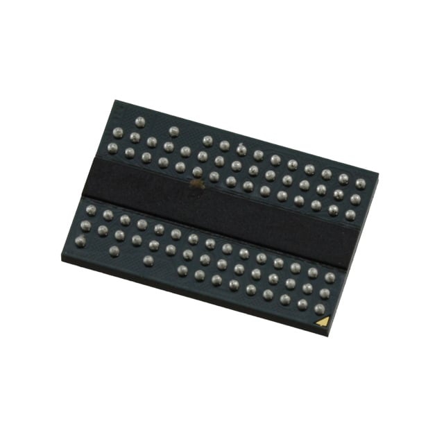
IS43DR16160A-3DBL
| Part Description |
IC DRAM 256MBIT PAR 84TWBGA |
|---|---|
| Quantity | 780 Available (as of June 15, 2026) |
| Product Category | Memory |
|---|---|
| Manufacturer | Integrated Silicon Solution Inc |
| Manufacturing Status | Obsolete |
| Manufacturer Standard Lead Time | Contact Us |
| Datasheet |
Specifications & Environmental
| Device Package | 84-TWBGA (8x12.5) | Memory Format | DRAM | Technology | SDRAM - DDR2 | ||
|---|---|---|---|---|---|---|---|
| Memory Size | 256 Mbit | Access Time | 450 ps | Grade | Commercial | ||
| Clock Frequency | 333 MHz | Voltage | 1.7V ~ 1.9V | Memory Type | Volatile | ||
| Operating Temperature | 0°C ~ 70°C (TA) | Write Cycle Time Word Page | 15 ns | Packaging | 84-TFBGA | ||
| Mounting Method | Volatile | Memory Interface | Parallel | Memory Organization | 16M x 16 | ||
| Moisture Sensitivity Level | 3 (168 Hours) | RoHS Compliance | ROHS Compliant | REACH Compliance | REACH Unaffected | ||
| Qualification | N/A | ECCN | EAR99 | HTS Code | 8542.32.0024 |
Overview of IS43DR16160A-3DBL – 256Mbit DDR2 SDRAM, 84-ball WBGA
The IS43DR16160A-3DBL is a 256 Mbit DDR2 SDRAM device organized as 16M × 16 with a parallel memory interface. It implements a double-data-rate architecture with on-chip features that support high-speed synchronous operation.
This device is intended for designs that require low-voltage (1.7 V–1.9 V) volatile system memory with programmable latency and burst options, delivered in an 84-ball WBGA package (8 × 12.5 mm).
Key Features
- Core & architecture Double-data-rate (DDR2) interface with 4-bit prefetch and on-chip DLL to align DQ and DQS transitions with CK. Supports differential data strobe (DQS / DQS̄) for synchronized data capture.
- Memory organization 256 Mbit capacity organized as 16M × 16 with 4 internal banks and programmable burst lengths of 4 or 8.
- Timing & performance Clock frequency specified at 333 MHz, access time of 450 ps, and write cycle time (word page) of 15 ns. Programmable CAS latency (CL) options include 3, 4, 5, and 6 plus programmable additive latency (AL) 0–5.
- Power & I/O Core and I/O supply range from 1.7 V to 1.9 V (VDD, VDDQ with 1.8 V ±0.1 V supported). JEDEC-standard 1.8 V I/O (SSTL_18-compatible).
- Signal integrity & drive control On-die termination (ODT) and adjustable data-output drive strength (full and reduced strength options) to help manage board-level signal integrity.
- Package & temperature 84-ball WBGA supplier package (84-TWBGA, 8 × 12.5 mm). Operating ambient temperature range specified as 0°C to 70°C (TA).
Typical Applications
- Embedded memory subsystems Used as parallel DDR2 SDRAM for embedded systems and controllers that require a 256 Mbit volatile memory with programmable timing and burst control.
- Consumer and industrial electronics Provides synchronous volatile storage where a 16M × 16 DDR2 organization and 84-ball WBGA package match board-level density and routing constraints.
- High-speed buffering Suited for designs requiring double-data-rate transfers and on-die features (DLL, ODT, differential DQS) to support synchronized high-speed data buffering.
Unique Advantages
- DDR2 double-data-rate throughput: Two data transfers per clock cycle via DDR2 architecture enable higher effective data rates compared with single-data-rate memories.
- Flexible timing configuration: Programmable CAS latency (CL 3–6) and additive latency (AL 0–5) let designers tune read/write timings to system requirements.
- On-die termination and drive control: ODT plus adjustable data-output drive strength help optimize signal integrity across different board topologies.
- Compact WBGA package: 84-ball (8 × 12.5 mm) WBGA package provides a small footprint for space-constrained PCBs while supporting parallel DDR2 connectivity.
- Low-voltage operation: 1.7 V–1.9 V supply range with JEDEC 1.8 V I/O compatibility supports modern low-voltage system designs.
Why Choose IS43DR16160A-3DBL?
The IS43DR16160A-3DBL positions itself as a compact, configurable DDR2 SDRAM option for systems that need 256 Mbit of parallel volatile memory with programmable timing, burst control, and on-die features such as DLL and ODT. Its low-voltage operation and adjustable drive strength make it adaptable to a range of board-level signal-integrity requirements.
This device is suited for engineers designing embedded subsystems, consumer or industrial electronics, and buffering applications that benefit from DDR2 performance and a small BGA footprint, providing a balance of performance, integration, and configurability for medium-density memory needs.
Request a quote or submit an inquiry for IS43DR16160A-3DBL to receive pricing and availability information tailored to your project requirements.


