IS43R16320D-5BL
| Part Description |
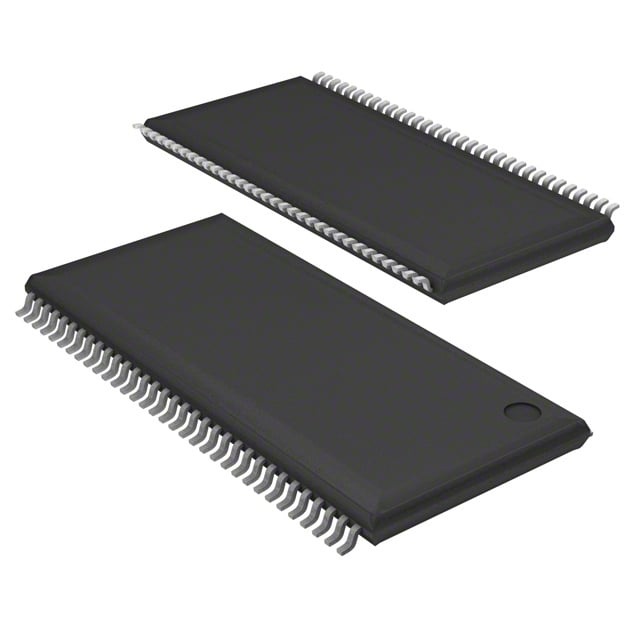
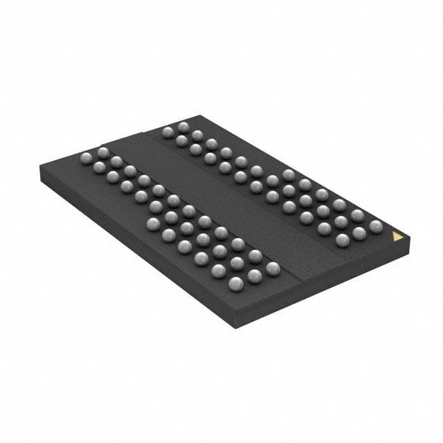
IC DRAM 512MBIT PAR 60TFBGA |
|---|---|
| Quantity | 1,021 Available (as of June 15, 2026) |

| Product Category | Memory |
|---|---|
| Manufacturer | Integrated Silicon Solution Inc |
| Manufacturing Status | Obsolete |
| Manufacturer Standard Lead Time | Contact Us |
| Datasheet |
Specifications & Environmental
| Device Package | 60-TFBGA (8x13) | Memory Format | DRAM | Technology | SDRAM - DDR | ||
|---|---|---|---|---|---|---|---|
| Memory Size | 512 Mbit | Access Time | 700 ps | Grade | Commercial | ||
| Clock Frequency | 200 MHz | Voltage | 2.5V ~ 2.7V | Memory Type | Volatile | ||
| Operating Temperature | 0°C ~ 70°C (TA) | Write Cycle Time Word Page | 15 ns | Packaging | 60-TFBGA | ||
| Mounting Method | Volatile | Memory Interface | Parallel | Memory Organization | 32M x 16 | ||
| Moisture Sensitivity Level | 3 (168 Hours) | RoHS Compliance | ROHS Compliant | REACH Compliance | REACH Unaffected | ||
| Qualification | N/A | ECCN | EAR99 | HTS Code | 8542.32.0028 |
Overview of IS43R16320D-5BL – 512Mbit DDR SDRAM, 60-TFBGA
The IS43R16320D-5BL is a 512‑Mbit DDR SDRAM organized as 32M × 16 with a parallel memory interface. It implements a double‑data‑rate architecture with on‑die DLL, differential clock inputs, and bidirectional data strobe (DQS) to support high‑speed read and write bursts.
With a maximum clock rate of 200 MHz (CL = 3), programmable CAS latencies, SSTL_2 compatible I/Os and four internal banks, this device targets designs that require deterministic, burst‑oriented DRAM performance in a compact 60‑TFBGA package operating from 0°C to 70°C.
Key Features
- Core Architecture Double‑data‑rate architecture with on‑die DLL and differential clock inputs (CK/CK̄) to align data and clock transitions for reliable high‑speed transfers.
- Memory Organization 512 Mbit capacity organized as 32M × 16 with four internal banks to enable concurrent bank operation and burst accesses.
- Data Interface Parallel DDR interface with bidirectional DQS; DQS is edge‑aligned for READs and centre‑aligned for WRITEs, and data/mask are referenced to both edges of DQS.
- Performance & Timing Supports burst lengths 2, 4 and 8, burst types sequential and interleave, programmable CAS latency 2 / 2.5 / 3, and a maximum clock frequency of 200 MHz (CL = 3) for the -5 speed grade.
- Power Supply voltage range specified at 2.5 V ~ 2.7 V; VDD and VDDQ options include tighter tolerances defined in the datasheet.
- Memory Management Auto Refresh and Self Refresh modes, Auto Precharge and T_RAS lockout support for standard DDR refresh and row management.
- Timing Characteristics Access time listed at 700 ps and write cycle/word page time of 15 ns as part of device timing specifications.
- Package & Temperature 60‑TFBGA (8 × 13) supplier device package with commercial operating temperature 0°C to +70°C.
- Device Options Family options include multiple data widths and packages (datasheet lists 16Mx32, 32Mx16, 64Mx8 configurations and lead‑free package availability).
Unique Advantages
- Deterministic burst performance: Programmable burst lengths and CAS latencies let designers tune latency and throughput to match system memory access patterns.
- DDR timing reliability: On‑die DLL, differential clock inputs, and DQS signaling provide engineered timing alignment for both reads and writes, reducing timing uncertainty at high data rates.
- Compact footprint: 60‑TFBGA (8×13) package concentrates 512 Mbit DDR in a small board area suitable for space‑constrained designs.
- Standard DDR interface: SSTL_2 compatible I/Os and parallel DDR signaling simplify integration with controllers that support standard DDR SDRAM interfaces.
- Flexible refresh and power modes: Auto Refresh and Self Refresh support helps manage power and data retention in systems that require periodic or extended refresh operations.
Why Choose IC DRAM 512MBIT PAR 60TFBGA?
The IS43R16320D-5BL positions itself as a practical DDR SDRAM option for systems requiring a 512‑Mbit parallel DDR memory with programmable latency and burst control. Its combination of DDR timing features (DQS, DLL, differential clocking), four internal banks, and SSTL_2 I/O compatibility provides predictable burst performance and straightforward integration into standard DDR memory controllers.
This device is suitable for designs that need compact, board‑level DDR memory with defined commercial temperature range and clear voltage/timing specifications, offering long‑term utility where consistent DDR behavior and package density are required.
Request a quote or submit an inquiry to receive pricing, availability, and ordering information for IS43R16320D-5BL.