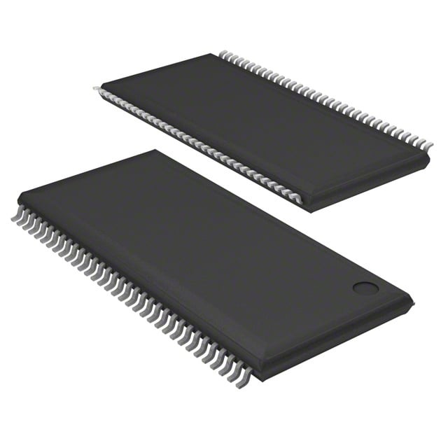
IS43R16320D-5TLI
| Part Description |
IC DRAM 512MBIT PAR 66TSOP II |
|---|---|
| Quantity | 387 Available (as of June 12, 2026) |

| Product Category | Memory |
|---|---|
| Manufacturer | Integrated Silicon Solution Inc |
| Manufacturing Status | Obsolete |
| Manufacturer Standard Lead Time | Contact Us |
| Datasheet |
Specifications & Environmental
| Device Package | 66-TSOP II | Memory Format | DRAM | Technology | SDRAM - DDR | ||
|---|---|---|---|---|---|---|---|
| Memory Size | 512 Mbit | Access Time | 700 ps | Grade | Industrial | ||
| Clock Frequency | 200 MHz | Voltage | 2.5V ~ 2.7V | Memory Type | Volatile | ||
| Operating Temperature | -40°C ~ 85°C (TA) | Write Cycle Time Word Page | 15 ns | Packaging | 66-TSSOP (0.400", 10.16mm Width) | ||
| Mounting Method | Volatile | Memory Interface | Parallel | Memory Organization | 32M x 16 | ||
| Moisture Sensitivity Level | 3 (168 Hours) | RoHS Compliance | ROHS3 Compliant | REACH Compliance | REACH Unaffected | ||
| Qualification | N/A | ECCN | EAR99 | HTS Code | 8542.32.0028 |
Overview of IS43R16320D-5TLI – IC DRAM 512MBIT PAR 66TSOP II
The IS43R16320D-5TLI from Integrated Silicon Solution Inc (ISSI) is a 512‑Mbit DDR SDRAM device organized as 32M × 16 with a parallel 16‑bit data interface. It implements double‑data‑rate architecture with two data transfers per clock cycle and is designed for systems requiring volatile high‑speed memory in a 66‑pin TSOP‑II footprint.
Key architecture elements include SSTL_2 compatible I/Os, differential clock inputs with DLL alignment, and four internal banks to support concurrent operations. The device targets designs needing up to 200 MHz clock operation (speed grade -5, CL=3) with VDD/VDDQ supply in the 2.5 V–2.7 V range and an industrial operating temperature range of -40°C to +85°C.
Key Features
- Memory Capacity & Organization 512 Mbit total capacity organized as 32M × 16, providing a 16‑bit parallel data path for burst read/write operations.
- DDR Architecture Double‑data‑rate operation performs two data transfers per clock cycle; supports burst lengths of 2, 4 and 8 with sequential and interleave burst types.
- Speed Grades & Timing Speed grade -5 supports clock frequencies up to 200 MHz (FCK max, CL=3). Programmable CAS latencies include 2, 2.5 and 3. Typical access timing includes 700 ps access time and write cycle time (word/page) of 15 ns.
- Interface & Signaling SSTL_2 compatible I/O with differential clock inputs (CK/CK̄) and bidirectional data strobe (DQS) for edge‑aligned READ and centre‑aligned WRITE data capture; data and commands referenced to clock and DQS edges.
- Internal Memory Management Four internal banks enable concurrent operation and pipelined Read/Write bursts; supports Auto Refresh and Self Refresh modes plus Auto Precharge.
- Power & Voltage VDD and VDDQ support 2.5 V ±0.2 V or 2.6 V ±0.1 V (device options), with supply range specified as 2.5 V–2.7 V in product data.
- Package & Temperature Delivered in a 66‑TSOP II (66‑TSSOP, 10.16 mm width) package. Operating temperature specified as -40°C to +85°C (TA).
Typical Applications
- Embedded system memory expansion Provides 512‑Mbit DDR SDRAM in a 16‑bit parallel interface for designs that require compact, board‑level high‑speed volatile memory.
- Buffering and frame memory Suitable where burst read/write access and pipelined DDR transfers are needed, leveraging DQS and DLL timing alignment for reliable data capture.
- Industrial electronics Industrial temperature rating to -40°C to +85°C for deployments in temperature‑challenging environments requiring 2.5 V class DDR memory.
Unique Advantages
- Compact TSOP‑II footprint: 66‑TSOP II package enables high density board layouts while providing a 16‑bit parallel data interface.
- SSTL_2 compatible I/O: Industry signaling compatibility simplifies interface design with SSTL_2‑based memory controllers and I/O systems.
- DDR pipelining and DQS timing: Bidirectional DQS with DLL alignment supports robust edge/cycle‑accurate data capture at doubled data rates.
- Flexible performance options: Programmable CAS latencies (2, 2.5, 3) and selectable burst lengths (2/4/8) allow designers to tune latency and throughput for target systems.
- Industrial temperature range: Specified operation from -40°C to +85°C for broader deployment in industrial applications.
- Low‑voltage supply: 2.5 V–2.7 V VDD/VDDQ operation reduces power domain complexity in systems designed around 2.5 V DDR signaling.
Why Choose IC DRAM 512MBIT PAR 66TSOP II?
The IS43R16320D-5TLI delivers a compact, standards‑oriented 512‑Mbit DDR SDRAM solution with SSTL_2 I/O, DLL‑aligned DQS, and flexible timing options—making it suitable for embedded and industrial designs that require predictable DDR performance in a 66‑pin TSOP‑II package. Its organization as 32M × 16 and four internal banks supports pipelined burst access patterns and concurrent memory operations.
This device is well suited to engineers specifying board‑level DDR memory with up to 200 MHz clock capability (speed grade -5, CL=3), 2.5 V class power rails, and an industrial temperature range. The combination of package density, signaling compatibility, and programmable timing provides a balance of performance and integration for space‑constrained systems.
Request a quote or contact sales to submit a quote for IS43R16320D-5TLI and to discuss volume availability, lead times, and technical support options.