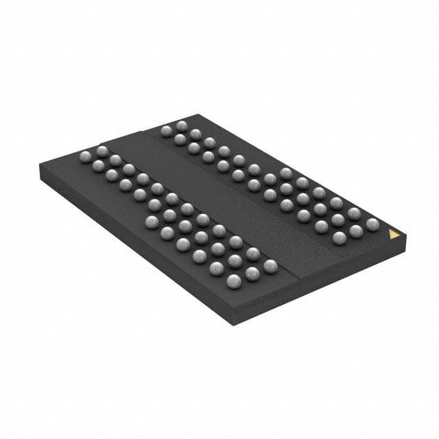
IS43R16320D-5BLI
| Part Description |
IC DRAM 512MBIT PAR 60TFBGA |
|---|---|
| Quantity | 596 Available (as of June 14, 2026) |
| Product Category | Memory |
|---|---|
| Manufacturer | Integrated Silicon Solution Inc |
| Manufacturing Status | Obsolete |
| Manufacturer Standard Lead Time | Contact Us |
| Datasheet |
Specifications & Environmental
| Device Package | 60-TFBGA (8x13) | Memory Format | DRAM | Technology | SDRAM - DDR | ||
|---|---|---|---|---|---|---|---|
| Memory Size | 512 Mbit | Access Time | 700 ps | Grade | Industrial | ||
| Clock Frequency | 200 MHz | Voltage | 2.5V ~ 2.7V | Memory Type | Volatile | ||
| Operating Temperature | -40°C ~ 85°C (TA) | Write Cycle Time Word Page | 15 ns | Packaging | 60-TFBGA | ||
| Mounting Method | Volatile | Memory Interface | Parallel | Memory Organization | 32M x 16 | ||
| Moisture Sensitivity Level | 3 (168 Hours) | RoHS Compliance | ROHS3 Compliant | REACH Compliance | REACH Unaffected | ||
| Qualification | N/A | ECCN | EAR99 | HTS Code | 8542.32.0028 |
Overview of IS43R16320D-5BLI – IC DRAM 512MBIT PAR 60TFBGA
The IS43R16320D-5BLI is a 512‑Mbit DDR SDRAM in a 60‑TFBGA (8×13) package organized as 32M × 16. It implements double‑data‑rate architecture with bidirectional data strobe (DQS) and on‑die DLL to align data and clock transitions for synchronous parallel memory operation.
Designed for systems that require a 512‑Mbit parallel DDR memory device, the device supports standard DDR features including SSTL_2‑compatible I/Os, programmable CAS latency and multiple burst modes, providing a configurable memory element for synchronous memory subsystems operating up to 200 MHz (FCK max, CL = 3).
Key Features
- Memory Architecture 512 Mbit DDR SDRAM organized as 32M × 16 with four internal banks to support concurrent operations and burst read/write sequences.
- DDR Data Handling Double‑data‑rate operation (two data transfers per clock) with bidirectional DQS; DQS is edge‑aligned for READs and center‑aligned for WRITEs.
- Clocking and DLL Differential clock inputs (CK/CK̅) and an on‑die DLL to align DQ/DQS transitions with clock transitions for reliable timing.
- Timing and Burst Control Programmable CAS latencies of 2, 2.5 and 3; burst lengths of 2, 4 and 8; sequential and interleave burst types; auto precharge and auto/self refresh support.
- Performance Supports FCK up to 200 MHz (Speed Grade -5, CL = 3) and an access time of 700 ps as specified.
- Interface Compatibility SSTL_2 compatible I/O signaling and parallel memory interface with data mask (DM) that masks write data on both edges of DQS.
- Power VDD and VDDQ operating range 2.5 V to 2.7 V (device -5 option specified at 2.6 V ± 0.1 V in datasheet options).
- Package and Temperature 60‑ball TFBGA (8×13) supplier device package; operating temperature specified as −40 °C to +85 °C (TA).
Typical Applications
- Parallel DDR Memory Subsystems For integration as a 512‑Mbit DDR memory device in synchronous parallel memory designs requiring SSTL_2 I/O.
- Buffered Data Storage Use where burst read/write buffering and programmable CAS latency are required to match system timing.
- Refresh‑Managed Memory Arrays Systems that utilize Auto Refresh and Self Refresh modes to maintain data integrity across refresh cycles.
Unique Advantages
- DDR Double‑Data‑Rate Architecture: Two data transfers per clock cycle increase effective throughput without increasing clock frequency.
- Flexible Timing Configuration: Programmable CAS latencies and multiple burst lengths enable tuning to system timing and performance needs.
- SSTL_2 Compatible I/O: Standard SSTL_2 signaling simplifies interface design with compatible memory controllers and I/O standards.
- On‑Die DLL and Differential Clock: DLL plus differential CK/CK̅ improve data/clock alignment for reliable capture of high‑speed DDR transfers.
- Industrial Temperature Range: Rated for −40 °C to +85 °C operation to support designs requiring wide ambient temperature tolerance.
Why Choose IS43R16320D-5BLI?
The IS43R16320D-5BLI is positioned as a configurable 512‑Mbit DDR SDRAM building block for parallel memory subsystems that require proven DDR features—DQS, DLL alignment, SSTL_2 I/O and programmable timing. With support for burst modes, multiple CAS latencies and four internal banks, the device provides the control and flexibility needed to match system timing and throughput targets.
This device is suited to designers needing a 32M × 16 DDR memory in a compact 60‑TFBGA package with a defined supply range (2.5 V–2.7 V) and industrial temperature operation. It offers scalability within DDR‑based designs where standard DDR signaling and refresh modes are required.
Request a quote or contact sales to discuss part availability, lead times, and volume pricing for IS43R16320D-5BLI.