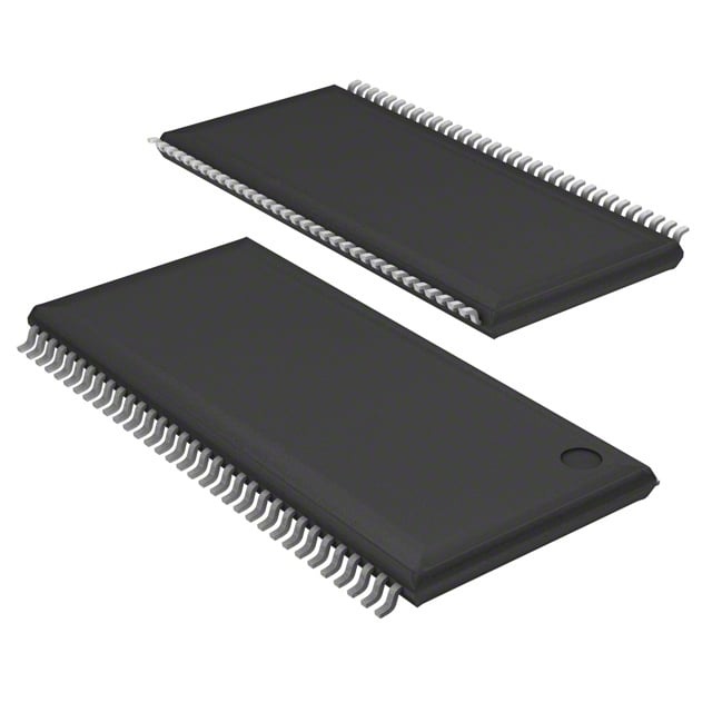
IS43R16320D-5TLI-TR
| Part Description |
IC DRAM 512MBIT PAR 66TSOP II |
|---|---|
| Quantity | 377 Available (as of June 10, 2026) |

| Product Category | Memory |
|---|---|
| Manufacturer | Integrated Silicon Solution Inc |
| Manufacturing Status | Obsolete |
| Manufacturer Standard Lead Time | Contact Us |
| Datasheet |
Specifications & Environmental
| Device Package | 66-TSOP II | Memory Format | DRAM | Technology | SDRAM - DDR | ||
|---|---|---|---|---|---|---|---|
| Memory Size | 512 Mbit | Access Time | 700 ps | Grade | Industrial | ||
| Clock Frequency | 200 MHz | Voltage | 2.5V ~ 2.7V | Memory Type | Volatile | ||
| Operating Temperature | -40°C ~ 85°C (TA) | Write Cycle Time Word Page | 15 ns | Packaging | 66-TSSOP (0.400", 10.16mm Width) | ||
| Mounting Method | Volatile | Memory Interface | Parallel | Memory Organization | 32M x 16 | ||
| Moisture Sensitivity Level | 3 (168 Hours) | RoHS Compliance | ROHS Compliant | REACH Compliance | REACH Unaffected | ||
| Qualification | N/A | ECCN | EAR99 | HTS Code | 8542.32.0028 |
Overview of IS43R16320D-5TLI-TR – IC DRAM 512MBIT PAR 66TSOP II
The IS43R16320D-5TLI-TR is a 512‑Mbit DDR SDRAM device organized as 32M × 16, implementing a pipeline double‑data‑rate architecture for high‑speed parallel memory operations. It integrates four internal banks, a DLL and DQS strobe support to align data transfers and enable reliable read/write capture.
This device targets systems requiring a compact 66‑TSOP II footprint with SSTL_2 compatible I/O and low‑voltage operation (2.5 V–2.7 V), delivering programmable latency, burst control and refresh modes to match a variety of performance and timing requirements.
Key Features
- Core & Architecture 512‑Mbit DDR SDRAM organized as 32M × 16 with four internal banks and pipeline architecture to support continuous read/write burst accesses.
- Memory & Performance Supports up to 200 MHz clock (speed grade -5, CL = 3) with programmable CAS latency (2, 2.5, 3), burst lengths 2/4/8 and an access time of 700 ps; write cycle time (word page) 15 ns.
- Interfaces & Timing SSTL_2 compatible I/O, differential clock inputs (CK/CK̄), bidirectional data strobe (DQS) with edge/center alignment, and a DLL to align DQ/DQS with clock transitions. Commands are registered on positive CK edges.
- Power & Voltage Operates from 2.5 V to 2.7 V (VDD/VDDQ) and supports VDD/VDDQ tolerance for the -5 speed grade as specified by the device.
- Refresh & Power Management Auto Refresh, Self Refresh and Auto Precharge modes are supported; Data Mask (DM) masks write data on both edges of DQS and TRAS lockout is supported.
- Package & Temperature Available in a 66‑TSOP II package (66‑TSSOP, 0.400" / 10.16 mm width) and specified for operation from -40°C to +85°C (TA).
Typical Applications
- High‑speed data buffering — Used where double‑data‑rate transfers and burst access (2/4/8) enable rapid buffering and throughput.
- Parallel‑interface memory subsystems — Provides 512‑Mbit storage with SSTL_2 compatible I/O and differential clock inputs for parallel DDR memory designs.
- Burst‑oriented data transfer engines — Programmable CAS latency and burst sequencing (sequential/interleave) support designs that optimize latency and throughput trade‑offs.
Unique Advantages
- Deterministic DDR timing: DLL, DQS strobe and differential clocks align data for consistent read/write timing and capture.
- Performance flexibility: Programmable CAS latency (2/2.5/3) and selectable burst lengths (2/4/8) allow tuning for different system timing requirements.
- Compact package footprint: 66‑TSOP II package (10.16 mm width) supports space‑constrained board designs without sacrificing capacity.
- Low‑voltage operation: 2.5 V–2.7 V VDD/VDDQ keeps power domain requirements compatible with SSTL_2 signaling.
- Robust refresh and power modes: Auto Refresh, Self Refresh and Auto Precharge options simplify memory maintenance and low‑power behavior.
- Industrial temperature range: Specified operation from -40°C to +85°C for designs requiring extended ambient tolerance.
Why Choose IC DRAM 512MBIT PAR 66TSOP II?
The IS43R16320D-5TLI-TR combines a 512‑Mbit DDR SDRAM organization with DDR architecture features—DLL, DQS, differential clocks and SSTL_2 I/O—to deliver configurable performance and reliable timing in a compact 66‑TSOP II package. Its programmable CAS latencies, burst modes and built‑in refresh options make it suitable for applications that require predictable DDR behavior and flexible timing tradeoffs.
This device is well suited for designers and procurement teams specifying a parallel DDR memory with 32M × 16 organization, industrial temperature capability and low‑voltage SSTL_2 signaling. Its mix of timing controls, refresh modes and compact packaging supports scalable designs where board space and deterministic memory timing are priorities.
Request a quote or submit an inquiry to receive pricing, availability and technical support for IS43R16320D-5TLI-TR.