IS43R32800D-5BI
| Part Description |
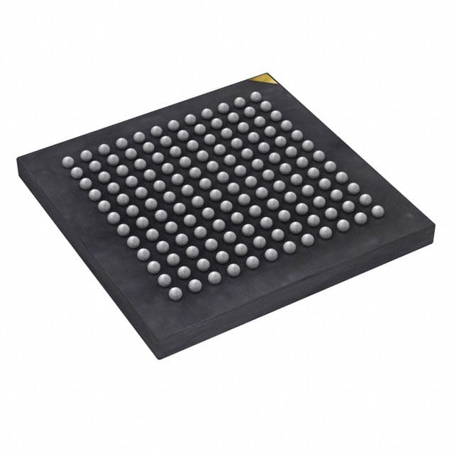
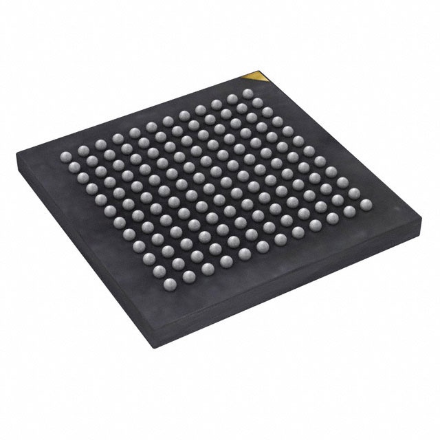
IC DRAM 256MBIT PAR 144LFBGA |
|---|---|
| Quantity | 1,287 Available (as of June 15, 2026) |
| Product Category | Memory |
|---|---|
| Manufacturer | Integrated Silicon Solution Inc |
| Manufacturing Status | Obsolete |
| Manufacturer Standard Lead Time | Contact Us |
| Datasheet |
Specifications & Environmental
| Device Package | 144-LFBGA (12x12) | Memory Format | DRAM | Technology | SDRAM - DDR | ||
|---|---|---|---|---|---|---|---|
| Memory Size | 256 Mbit | Access Time | 700 ps | Grade | Industrial | ||
| Clock Frequency | 200 MHz | Voltage | 2.3V ~ 2.7V | Memory Type | Volatile | ||
| Operating Temperature | -40°C ~ 85°C (TA) | Write Cycle Time Word Page | 15 ns | Packaging | 144-LFBGA | ||
| Mounting Method | Volatile | Memory Interface | Parallel | Memory Organization | 8M x 32 | ||
| Moisture Sensitivity Level | 3 (168 Hours) | RoHS Compliance | ROHS3 Compliant | REACH Compliance | REACH Unaffected | ||
| Qualification | N/A | ECCN | EAR99 | HTS Code | 8542.32.0024 |
Overview of IS43R32800D-5BI – IC DRAM 256MBIT PAR 144LFBGA
The IS43R32800D-5BI is a 256 Mbit DDR SDRAM organized as 8M × 32 bits in a 144‑LFBGA (12×12) package. It implements a double‑data‑rate pipeline architecture with four internal banks, differential clock inputs and a DLL to align data and strobe timing for reliable high‑speed transfers.
This parallel DDR memory device is suited for designs requiring a 256‑Mbit volatile memory with SSTL_2 compatible I/O, a 2.3 V–2.7 V supply range, and an operating temperature range of −40 °C to +85 °C. Key value propositions include predictable timing (up to 200 MHz Fck for the -5 speed grade), programmable CAS latency and support for auto/self refresh modes.
Key Features
- Core Architecture 8M × 32 internal organization with four internal banks enables pipelined read/write burst operation and concurrent bank activity.
- DDR SDRAM Operation Double‑data‑rate architecture supports two data transfers per clock cycle with programmable burst lengths of 2, 4 and 8 and burst types sequential or interleave.
- Data Path and Timing Bidirectional data strobe (DQS) is transmitted/received with data (edge‑aligned for reads, center‑aligned for writes). Differential clock inputs (CK/¯CK) and on‑die DLL align DQ/DQS with clock transitions.
- I/O and Interface SSTL_2 compatible I/O standard and parallel memory interface with data mask (DM) that masks write data on both edges of DQS.
- Performance and Timing -5 speed grade supports Fck up to 200 MHz; programmable CAS latencies of 2, 2.5 and 3; example timing includes a write cycle/word page time of 15 ns and access time of 700 ps.
- Power VDD and VDDQ operate at 2.5 V ± 0.2 V (specified range 2.3 V to 2.7 V).
- Reliability and Refresh Supports Auto Refresh, Self Refresh and Auto Precharge modes; TRAS lockout (tRAP = tRCD) is supported.
- Package and Temperature Available in a 144‑ball LFBGA (12×12) package with an operating temperature range of −40 °C to +85 °C (TA).
Typical Applications
- Embedded Systems Suitable as system DDR memory where a 256‑Mbit parallel DDR SDRAM is required for temporary data storage and buffering.
- Consumer Electronics Used for volatile memory needs in devices that require DDR SDRAM with programmable CAS latency and burst operation.
- Industrial Equipment Applicable in industrial designs that require operation across −40 °C to +85 °C and a compact 144‑LFBGA package.
Unique Advantages
- Deterministic DDR timing: Programmable CAS latency (2, 2.5, 3), DLL alignment and DQS support provide precise timing control tied directly to the device’s Fck limits.
- Flexible burst operation: Burst lengths of 2, 4 and 8 with sequential and interleave options allow matching access patterns to system requirements.
- SSTL_2 compatible I/O: Ensures signal compatibility with SSTL_2 interfaces at the specified supply range (VDD/VDDQ = 2.5 V ±0.2 V).
- Compact BGA package: 144‑ball LFBGA (12×12) provides high density in a small footprint for space‑constrained boards.
- Wide operating range: Specified operation from −40 °C to +85 °C supports deployment in temperature‑variable environments.
Why Choose IS43R32800D-5BI?
The IS43R32800D-5BI combines a 256‑Mbit DDR SDRAM organization with DDR pipeline architecture, on‑die DLL, DQS timing support and SSTL_2 I/O to deliver predictable, programmable memory timing for systems requiring parallel DDR memory. Its -5 speed grade capability (up to 200 MHz Fck), programmable CAS latencies and burst modes make it suitable for designs that need controlled, repeatable DDR behavior.
This device is well matched to designers and procurement teams seeking a compact 144‑LFBGA packaged DRAM with defined voltage and temperature ranges, refresh modes and timing parameters documented for integration into embedded, consumer or industrial applications.
Request a quote or contact sales to discuss availability, lead times and pricing for the IS43R32800D-5BI.