IS43R32800D-5BLI
| Part Description |
IC DRAM 256MBIT PAR 144LFBGA |
|---|---|
| Quantity | 1,143 Available (as of June 17, 2026) |

| Product Category | DRAM Memory |
|---|---|
| Manufacturer | Integrated Silicon Solution Inc |
| Manufacturing Status | Active |
| Manufacturer Standard Lead Time | 8 Weeks |
| Datasheet |
Specifications & Environmental
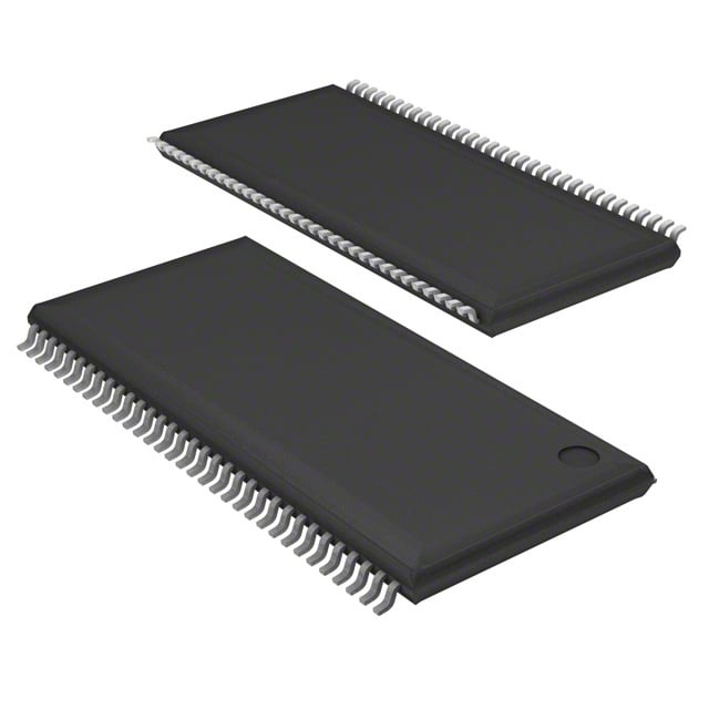
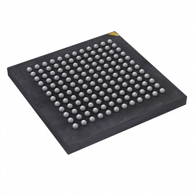
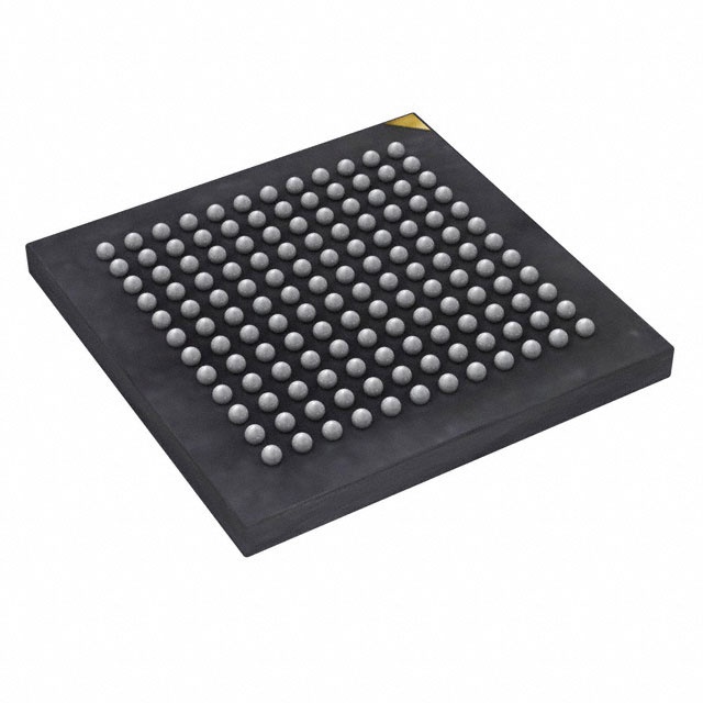
| Device Package | 144-LFBGA (12x12) | Memory Format | DRAM | Technology | SDRAM - DDR | ||
|---|---|---|---|---|---|---|---|
| Memory Size | 256 Mbit | Access Time | 700 ps | Grade | Industrial | ||
| Clock Frequency | 200 MHz | Voltage | 2.3V ~ 2.7V | Memory Type | Volatile | ||
| Operating Temperature | -40°C ~ 85°C (TA) | Write Cycle Time Word Page | 15 ns | Packaging | 144-LFBGA | ||
| Mounting Method | Volatile | Memory Interface | Parallel | Memory Organization | 8M x 32 | ||
| Moisture Sensitivity Level | 3 (168 Hours) | RoHS Compliance | ROHS3 Compliant | REACH Compliance | REACH Unaffected | ||
| Qualification | N/A | ECCN | EAR99 | HTS Code | 8542.32.0024 |
Overview of IS43R32800D-5BLI – IC DRAM 256MBIT PAR 144LFBGA
The IS43R32800D-5BLI is a 256‑Mbit DDR SDRAM organized as 8M × 32 with a parallel 32‑bit interface in a 144‑LFBGA (12 × 12) package. It implements a double‑data‑rate architecture with on‑die DLL, differential clock inputs and SSTL_2 compatible I/O for high‑rate synchronous memory transfers.
This device targets designs requiring a compact 256‑Mbit DDR memory element with programmable timing and burst options and supports industrial temperature operation from −40°C to +85°C and a supply range of 2.3 V to 2.7 V.
Key Features
- Memory Architecture — 256 Mbit DDR SDRAM organized as 8M × 32 with four internal banks to allow concurrent operations and efficient burst transfers.
- High‑speed DDR Operation — Double‑data‑rate architecture providing two data transfers per clock cycle; specified maximum clock frequency up to 200 MHz (speed grade -5).
- Programmable Timing — Programmable CAS latency options (2, 2.5 and 3) and selectable burst lengths (2, 4, 8) with sequential and interleave burst types.
- Data Integrity & Timing — Bidirectional data strobe (DQS) transmitted/received with data; DQS edge‑aligned for READs and center‑aligned for WRITEs; on‑die DLL aligns DQ/DQS to CLK.
- Interface & Commands — Differential clock inputs (CK/CK̄); commands registered on the positive edge of CLK; data and data mask referenced to both edges of DQS.
- Write Mask & Burst Control — Data Mask (DM) masks write data on both rising and falling edges of the data strobe; Auto Precharge, Auto Refresh and Self Refresh modes supported.
- Power & Voltage — VDD and VDDQ nominal 2.5 V ± 0.2 V with an operating supply range of 2.3 V to 2.7 V; I/Os are SSTL_2 compatible.
- Performance & Timing Parameters — Access time 700 ps; write cycle time (word/page) 15 ns; key timing parameters documented for speed grades including -5 (200 MHz).
- Package & Temperature — 144‑ball LFBGA package (12 × 12 mm); industrial temperature range −40°C to +85°C supported.
Typical Applications
- Embedded memory subsystems — Provides a compact 256‑Mbit DDR element for systems that require a 32‑bit parallel DDR SDRAM component.
- High‑speed buffering and frame storage — Double‑data‑rate transfers, programmable burst lengths and CAS latency options make it suitable for designs needing predictable burst performance.
- Industrial equipment — Rated for −40°C to +85°C operation to address industrial temperature environments where this memory density and form factor are required.
Unique Advantages
- DDR data throughput — Double‑data‑rate architecture and differential clocking deliver two data transfers per clock for higher effective bandwidth within the specified 200 MHz clock rating.
- Flexible timing configuration — Programmable CAS latencies and multiple burst lengths allow tuning of latency and burst behavior to match system timing requirements.
- SSTL_2 compatible I/O — Standard SSTL_2 I/O levels simplify interfacing with SSTL_2 memory controllers and board designs operating at nominal 2.5 V.
- Robust timing control — On‑die DLL plus DQS edge/center alignment supports reliable data capture on both read and write operations.
- Compact LFBGA package — 144‑ball 12 × 12 LFBGA provides a small footprint for space‑constrained boards while delivering a 32‑bit parallel data path.
- Industrial temperature support — Operation from −40°C to +85°C addresses thermal requirements for a range of industrial applications.
Why Choose IC DRAM 256MBIT PAR 144LFBGA?
The IS43R32800D-5BLI delivers a 256‑Mbit DDR SDRAM option with configurable timing, SSTL_2 I/O compatibility and on‑die timing support for reliable, high‑rate parallel memory operation. Its 8M × 32 organization, four internal banks and burst/CAS programmability provide designers with the flexibility to optimize throughput and latency for targeted system needs.
This device is suitable for designs that require a compact 144‑LFBGA memory package, 32‑bit parallel data paths, and industrial temperature operation. The documented voltage, timing and functional features make it appropriate for systems that must balance footprint, speed and deterministic DDR behavior.
Request a quote or submit an inquiry to check availability, lead times and pricing for the IS43R32800D-5BLI.