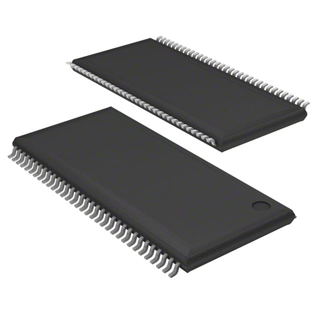
IS43R83200B-5TL
| Part Description |
IC DRAM 256MBIT PAR 66TSOP II |
|---|---|
| Quantity | 733 Available (as of June 15, 2026) |
| Product Category | Memory |
|---|---|
| Manufacturer | Integrated Silicon Solution Inc |
| Manufacturing Status | Obsolete |
| Manufacturer Standard Lead Time | Contact Us |
| Datasheet |
Specifications & Environmental
| Device Package | 66-TSOP II | Memory Format | DRAM | Technology | SDRAM - DDR | ||
|---|---|---|---|---|---|---|---|
| Memory Size | 256 Mbit | Access Time | 700 ps | Grade | Commercial | ||
| Clock Frequency | 200 MHz | Voltage | 2.3V ~ 2.7V | Memory Type | Volatile | ||
| Operating Temperature | 0°C ~ 70°C (TA) | Write Cycle Time Word Page | 15 ns | Packaging | 66-TSSOP (0.400", 10.16mm Width) | ||
| Mounting Method | Volatile | Memory Interface | Parallel | Memory Organization | 32M x 8 | ||
| Moisture Sensitivity Level | 3 (168 Hours) | RoHS Compliance | ROHS3 Compliant | REACH Compliance | REACH Unaffected | ||
| Qualification | N/A | ECCN | EAR99 | HTS Code | 8542.32.0024 |
Overview of IS43R83200B-5TL – IC DRAM 256MBIT PAR 66TSOP II
The IS43R83200B-5TL is a 256 Mbit double data rate (DDR) synchronous DRAM organized as 32M × 8. It implements a parallel SSTL_2 interface and DDR architecture that performs two data transfers per clock cycle.
Designed for systems that require low-voltage DDR memory with programmable timing and burst options, the device supports clock rates up to 200 MHz and comes in a compact 66-TSSOP (TSOP II) package for board-level integration within commercial temperature environments.
Key Features
- DDR Synchronous Architecture Double data rate operation delivers two data transfers per clock cycle for increased throughput compared to single data rate DRAM.
- Memory Organization 256 Mbit capacity organized as 32M × 8 provides a standard byte-wide DRAM configuration for parallel memory systems.
- Clock and Timing Supports clock frequencies up to 200 MHz with access time specified around ±0.70 ns and programmable CAS latencies (2.0 / 2.5 / 3.0) and burst lengths (2 / 4 / 8).
- Data Strobe and Clocking Bidirectional data strobe (DQS) and differential clock inputs (CLK and /CLK) with a DLL that aligns DQ/DQS transitions to CLK edges.
- Memory Banking and Refresh 4-bank architecture (BA0, BA1) with 8192 refresh cycles per 64 ms and support for auto refresh and self refresh modes.
- Addressing and Burst Control Row addresses A0–A12 and column addresses A0–A9 (×8) enable standard DDR row/column operations with auto precharge and all-bank precharge control via A10.
- Low-Voltage Supply Operates from 2.3 V to 2.7 V (nominal VDD = 2.5 V), supporting low-voltage system designs.
- Package Available in a 66-pin TSOP II (66-TSSOP) package with 0.400" (10.16 mm) width for compact board-level integration.
- Commercial Temperature Range Rated for 0°C to +70°C ambient operation.
- Write and Cycle Timing Word/page write cycle time specified at 15 ns to support typical DDR write operations.
Typical Applications
- Embedded DDR Memory Use as on-board parallel DDR DRAM where a 256 Mbit, 32M × 8 configuration and SSTL_2 interface are required.
- High-speed Buffering Suitable for buffer or temporary storage roles that leverage DDR transfers, 4-bank operation and programmable burst behavior to manage high-throughput bursts.
- Commercial Electronics Integration into commercial-temperature-range products that need a low-voltage DDR memory solution with standard row/column addressing.
Unique Advantages
- Double Data Rate Throughput: Two data transfers per clock cycle enable higher effective data rates compared to single data rate DRAM.
- Flexible Timing Control: Programmable CAS latencies and burst lengths let designers tune performance and latency to match system requirements.
- Standard SSTL_2 Interface: Differential clocking and SSTL_2 signaling simplify integration with systems expecting standard DDR parallel memory interfaces.
- Low-Voltage Operation: 2.3 V–2.7 V supply range reduces power domain requirements and supports low-voltage memory designs.
- Compact TSOP II Package: 66-TSSOP (0.400", 10.16 mm) package provides a compact footprint for space-constrained board layouts.
- Robust Refresh and Banking: 4-bank architecture with 8192 refresh cycles/64 ms and auto/self refresh options supports continuous operation and predictable refresh behavior.
Why Choose IC DRAM 256MBIT PAR 66TSOP II?
The IS43R83200B-5TL positions itself as a straightforward, low-voltage DDR memory component offering 256 Mbit capacity, programmable timing options and standard SSTL_2 parallel interface. Its support for up to 200 MHz clocking, coupled with a 4-bank architecture and DLL-aligned data strobe, makes it suitable for designs that require synchronous DDR performance in a compact TSOP II package.
Engineers designing commercial-temperature systems that need a byte-wide (×8) DDR DRAM with flexible burst and latency control will find the IS43R83200B-5TL aligns to common DDR subsystem requirements while maintaining a small footprint and low-voltage operation.
Request a quote or submit a request for pricing and availability for the IS43R83200B-5TL to obtain lead-time and ordering information.